AE Card
This card specifies an excitation at an edge between triangular surface elements.
On the Source/Load tab, in the Sources group,
click the ![]() Voltage source
icon. From the drop-down list, click the
Voltage source
icon. From the drop-down list, click the ![]() Voltage on edge (AE) icon.
Voltage on edge (AE) icon.

Parameters:
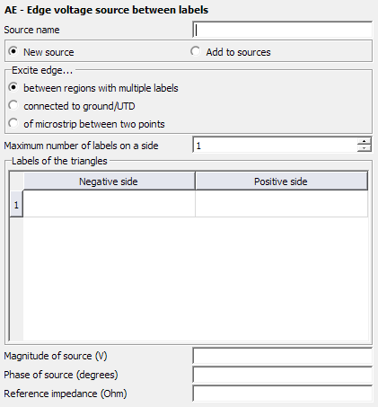
- New source
- A new excitation is defined which replaces all previously defined excitations.
- Add to sources
- A new excitation is defined which is added to the previously defined excitations.
- Excite edge on a defined port
- The name of the referenced port defined using a PT card.
- Excite edge between regions with multiple labels (old format)
- The excitation is placed on the edge between the regions with labels specified in Negative side and Positive side. Use the field Maximum number of labels on a side to increase the number of rows available in the table. The positive source direction is from the Negative side towards the Positive side.
- Excite edge connected to ground/UTD (old format)
- Excite the edges of metallic triangles with the labels specified in the Negative side or Positive side. The edges of these triangles are connected to UTD surfaces or to a PEC ground plane (as specified with a BO or GF card).
- Excite edge of microstrip between two points (old format)
- This is a special microstrip line feed. The excitation is placed on all edges on a
line between points (previously specified with DP cards). The points are specified in
the Start point of edge and End point of
edge dialogs. A GF card with a conducting ground must be present.Note: The dialog layout and visibility of options will differ according to the selection in the Excite edge group.
- Meshed surface represents positive feed side
- By default, the feed direction is such that the meshed surface represents the negative feed side. The vector direction of the current is then towards the UTD or ground. When this option is checked, the feed orientation is reversed.
- Magnitude of source (V)
- Magnitude value of the voltage source in V.
- Phase of source (degrees)
- Phase of the voltage source in degrees.
- Reference impedance (Ohm)
- The reference impedance of the excitation is used for S-parameter calculations and is the reference impedance used for realised gain calculations. It is also the default reference impedance used to calculate and display the reflection coefficient in POSTFEKO. If this field is empty or 0 in an S-parameter calculation, the value specified at the SP card is used. For realised gain and reflection coefficient calculations, 50 Ohm will be assumed when the field is empty or 0.
It should be noted that the edge between the surfaces with labels Negative side and Positive side does not have to be straight. It is possible, for example, to excite two half cylinders against each other. If an impedance must also be applied to the edge, the AE card can be combined with the LE card.
For the case where
the option, between regions with multiple labels, is selected more
than two surfaces may be connected to a feed edge. Examples for this as seen in the figures
are:
- one surface fed against three others
- two surfaces fed against two other surfaces
- and a feeding edge on a junction between three surfaces.


