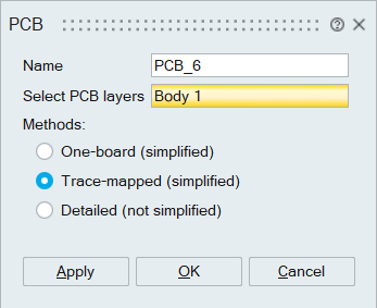
PCB
![]()
Introduction
PCB smart object provides
three different options to model the PCB in a thermal simulation.
- It is important to create key planes to capture the layers properly for Trace-Map and Detailed method
- Users should make sure that the value of the parameter “Minimum distance between key planes” in “Geometry Discretization” should be less than the minimum Cu layer thickness
One- board (Simplified)
- In this method in plane and through plane thermal properties are calculated for the board based on a thermal resistance network of Cu and FR4 layers.
- The orthotropic properties will be same across the board.
- This method is useful in a system level simulation where the localised effect due to the presence of Cu trances is ignored.
Trace - mapped (Simplified)
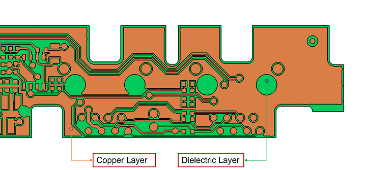
- In this methos each copper trace layer is merged with the attached FR4 substrate
forming a layer of a homogeneous material with averaged properties.
- The effective density, specific heat, and orthotropic thermal conductivity are
respectively calculated as
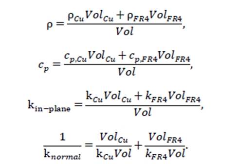
Here, 𝑉𝑜𝑙=𝑉𝑜𝑙𝐶𝑢+𝑉𝑜𝑙𝐹𝑅4 is the sum of the in-c ell volumes of the conductive and dielectric material and the subscript normal denotes the heat conduction perpendicular to the plane of the corresponding PCB layer
-
This method is also used in a system level thermal simulation where more accuracy is needed.
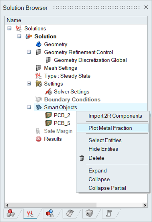
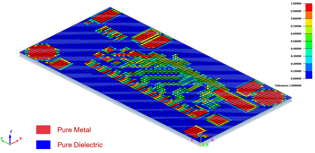
- The resulting metal fraction for the PCB can be displayed by right-clicking “Smart Objects” in the Solution Browser and selecting “Plot Metal Fraction”:
Detailed (Not Simplified)
- In this methos the Cu and FR4 layers are preserved by creating mesh for them.
- This method must be used to calculate the Joules heating in the Cu traces due to the flow of Current. Users need to apply current and voltage boundary conditions for the same.
- This method is recommended to use in a PCB level simulation where a higher degree of accuracy is needed across the board.