PCB Outline Spacing
Verify the clearance between a single board outline and various objects.
The PCB Outline Spacing dialog contains the following
sections:
- FPCB Layer Definition: Set the FPCB layer to distinguish between the FPCB
and Rigid PCB layer. With Rigid-Flex PCB, Rigid PCB is stacked based on the
FPCB layer.
- FPCB Layer Name Filter: Set the FPCB layer using the
String Filter dialog.
- Layer Name: Recognize the FPCB Layer based on the layer name.
- Layer Comment: Recognize the FPCB Layer based on the layer comment.
- FPCB Layer Name Filter: Set the FPCB layer using the
String Filter dialog.
- Laser Via Definition: Define a laser via.
- Maximum Hole Size: Define the via with maximum hole size that same and smaller holes will be recognized as a layer via.
- Padstack List: Select the via using padstack name.
- Padstack String: Define the via using string filter.
- PCB’s Outline: Select the measuring base for verifying the distance from the
board outline.
- From Line Edge
- From Line Center
-
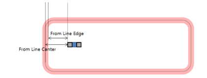
Figure 1. - Copper-Pour Clearance: Verify the clearance between the board outline and
copper-pour data.
- Clearance: Set the clearance value.
- Clearance for FPCB Layer: Set the clearance value for the FPCB Layer.
- Clearance for Figure Object: Check the clearance for the figure objects.
- Routing Pattern Clearance: Verify the clearance between the board outline
and routing patterns.
- Clearance: Set the clearance value.
- Clearance for FPCB Layer: Set the clearance value for the FPCB Layer.
- Exclude Checking for JTAG Component Connected Pattern: Skip the analysis for the routing nets that connect to a defined JTAG component.
- Clearance for Figure Object: Check the clearance for the figure objects.
- Via Clearance: Verify the clearance between the board outline and specified
vias.
- Common Via Clearance: Verify the clearance between the board outline
and specified vias.
- Board Outline to Via in Copper-Pour: Set the clearance value between the board outline and vias in the copper-pour.
- Board Outline to Via in Routing Pattern: Set the clearance value between the board outline and vias in the routing pattern.
- Board Outline to Via in Copper-Pour for FPCB Layer: Set the clearance value between the board outline and vias in the copper-pour on the FPCB Layer.
- Board Outline to Via in Routing Pattern for FPCB Layer: Set the clearance value between board outline and vias in the routing pattern located on the FPCB Layer.
- Laser Via Definition: Verify the clearance between the board outline
and laser vias
- Maximum Via Hole Size: Set the maximum via hole size.
- Via Library: Select the laser via from the library list.
- Laser Via Clearance: Check the clearance between the board
outline and laser vias.
- Board Outline to Laser Via in Copper-Pour: Set the clearance value between the board outline and laser vias in a copper-pour.
- Board Outline to Laser Via in Routing Pattern: Set the clearance value between the board outline and laser vias in a routing pattern.
- Board Outline to Laser Via in Copper-Pour for FPCB Layer: Set the clearance value between the board outline and laser vias in a copper-pour located on the FPCB Layer.
- Board Outline to Laser Via in Routing Pattern for FPCB Layer: Set the clearance value between the board outline and laser vias in the routing pattern on the FPCB Layer.
- Clearance for Figure Object: Check the clearance for the figure objects.
- Common Via Clearance: Verify the clearance between the board outline
and specified vias.
- Component Clearance: Verify the clearance between the board outline and
specified components.
- Target Components’ Placed Layer: Select the layer that the specified component is located on.
- Component Groups & Clearance:
- Item: Specify the item name.
- Component Group: Select the target component group from the list.
- Measure Base: Set the target component measurement base.
- Filter: Select an inequality sign for the clearance between the target component and the PCB outline.
- Clearance: Set the clearance value between the specified components and the PCB Outline.
- Horizontal Clearance: Set the horizontal clearance value between the PCB outline segment and specified components.
- Vertical Clearance: Set the vertical clearance value between
the PCB outline segment and specified components.
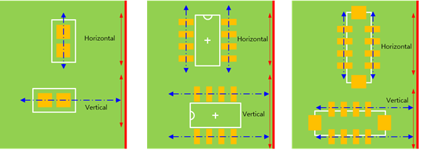
Figure 2.
- Exceptional Component: Select the component group to exclude during analysis.
- Except for SMD Component Pins, having no Metal Mask: Exclude pins that do not have a metal mask from analysis.
- Clearance to Remainder Components: Set the clearance value for the undefined components in the table in Component Groups & Clearance.
- Horizontal/Vertical Clearance to Remainder Components: Set the
horizontal and vertical clearance value for the undefined components
in the table in Component Groups & Clearance.
Figure 3.
- Component Pin’s Clearance: Verify the clearance between the board outline
and the component pin or board figure shape pads.
- Target Component Group: Select the target component group.
- SMD Type Pin: Set the clearance value between the board outline and SMD pin.
- SMD Type Figure Pad: Set the clearance value between the board outline and the SMD type board figure shape pad.
- DIP Type Pin: Set the clearance value between the board outline and DIP pin.
- DIP Type Figure Pad: Set the clearance value between the board outline and the DIP type board figure shape pad.
- Components Close to Board Outline: Verify components placed too far away
from the board outline.
- Component Group: Set the components that should be placed closely to the board outline.
- Measure Base: Set the component measurement base for verifying the distance from the board outline.
- Maximum Distance from Board Outline: Set the maximum allowable distance value for the components and the board outline.
- Silk Screen Clearance: Verify the clearance between the board outline and
silkscreen.
- Set Silkscreen Text Line Width as Zero: Ignore the text silkscreen width to verify the clearance to the silkscreen data.
- Component Text: Set the clearance value between the board outline and the component text.
- Component Figure: Set the clearance value between the board outline and the component figure geometries.
- Board Text: Set the clearance value between the board outline and the board text.
- Board Figure: Set the clearance value between the board outline and the board figure geometries.
- Guard Silk Screen Width Checking: Verify the clearance between the board
outline and the guard silkscreen.
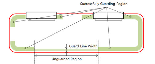
Figure 4.- Target Layer: Select the target layer where the guard silkscreen should be designed.
- Minimum Guarding Ratio (%): Select the minimum guarding ratio
regarding the board outline.
- Minimum Silkscreen Width: Set the minimum silkscreen width to accept as the guard silkscreen.
- Components Compulsory Include into Guard Area: Set the region occupied by specified components like connectors to accept as the guarding area.
- Metal Mask Clearance: Verify the clearance between the board outline and the
metal mask.
- Component Metal Mask: Set the clearance value between the board outline and the component metal mask.
- Board Metal Mask: Set the clearance value between the board outline and the board metal mask.
- Solder Mask Checking: Verify the clearance between the board outline and the
solder mask.
- PCB’s Outline: Select the measuring base for verifying the distance
from the board outline. Select a method between From Line Edge or
From Line Center.
Figure 5. - Component Group: Select the target component group from the list.
- Clearance: Set the clearance value between the component solder mask and the board outline.
- Board Figure Clearance: Set the clearance value between the board outline and the board figure solder mask.
- PCB’s Outline: Select the measuring base for verifying the distance
from the board outline. Select a method between From Line Edge or
From Line Center.
- Solder Mask check the inner side of the PCB Outline
- Target Layer
- Top Layer : Solder Mask exists on the Top Layer.
- Bottom Layer : Solder Mask exists on the Bottom Layer.
- All Layer : Solder Mask exists on the Top and Bottom Layer.
- Minimum distance between Solder Mask edge to PCB Outline.
- Target Layer