Guide Hole
Validate the guiding hole in the PCB's design.
The Guide Hole dialog contains the following sections:
- Board Direction Definition: Decide the board's placement status using the
soldering mark or by defining the soldering direction.
- Soldering-Mark Component Group: Define the soldering mark. Use if it is registered as a group of components.
- Mark Direction: Define the mark’s direction and the soldering
direction.
Figure 1. 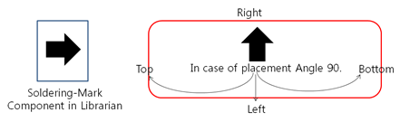
- Soldering Direction: Define the direction of the board without using
soldering-mark case.
Figure 2. 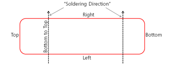
- Guide Hole Definition: Define the target guiding hole to analyze.
- Component Group Selection: Select the component group from Component group list. Use if a component is used as a guiding hole.
- Padstack String: Define the via using string filter. Use if a
padstack is used as a guiding hole.
- Import(.txt): Apply Filter Type based on the characters
entered in the .txt file.
- Apply as a prefix when (|F|) ABC is entered in the .txt file.
- Apply as a mid-string when ABC is entered in the .txt file.
- Apply as a suffix when ABC(|P|) is entered in the .txt file.
- Export(.txt): Export the characters registered in the String Item in .txt file format.
- Import(.txt): Apply Filter Type based on the characters
entered in the .txt file.
- Via (NPTH): Set the via from the via list. Use if a via is used as a guiding hole.
- Board Figure Geometries: Define the hole length and diameter. Use if
board figure geometries are used as a guide hole.
Figure 3. 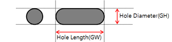
- Guide Hole Searching Ranges from Board Corner: Set the area where the
guiding hole is located. Specify area values with dX and dY from the board
corners. Refer to Figure 4.
Figure 4. Guide Hole Searching Ranges from the Board Corner 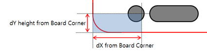
- Guide Hole Size Check: Verify the guide hole size. If set to Value, it will
be detected as Fail if it does not match the specified value. If set to
Range, it will be detected as Fail if it is not within the defined range.
- Guide Hole Diameter: Verify the diameter of the guide hole.
- Guide Hole Length: Verify the length of the guide hole.
- Circle Type Guide Hole Checking
- Circle Guide Hole Counting: Verify the number of circle type guide
holes at specified regions.
Figure 5. 
- Number of Total Guide Hole: Verify the number of guide holes.
- Counting: Verify the number of guide holes in the upper and lower side of the PCB.
- Diagonal Counting: Verify the number of guide holes in the
diagonal sides.
- Left Top, Right Bottom: Set the number of guide holes in these regions.
- Right Top, Left Bottom: Set the number of guide holes in these regions.
- Circle Type Guide Hole Location: Verify the guide holes in each
board corner. The table rows each correspond with the four corners
of the PCB.
Figure 6. 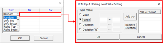
Figure 7. 
- Circle Guide Hole Counting: Verify the number of circle type guide
holes at specified regions.
- Center Guide Hole Checking
- Major Axis Existence: Verify the center guide hole is on the major axis of the board.
- Minor Axis Existence: Verify the center guide hole is on the minor axis of the board.
- Tolerance: Input the tolerance value from the center of the boards major or minor axis.
- Check Single Guide Hole: Verify there is only one center guide hole.
- Ellipse Type Guide Hole Checking
- Ellipse Guide Hole Counting: Verify the number of ellipse type guide
holes at specified regions.
Figure 8. 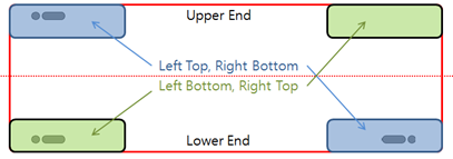
- Number of Total Guide Hole: Verify the number of guide holes.
- Counting: Verify the number of guide holes for the upper and lower side of the PCB.
- Diagonal Counting: Verify the number of guide holes at the
diagonal sides of the PCB.
- Left Top, Right Bottom: Set the number of guide holes in these regions.
- Right Top, Left Bottom: Set the number of guide holes in these regions.
- Ellipse Type Guide Hole Location: Verify there are guide holes in
each corner. The table rows each correspond with the four corners of
the PCB.
Figure 9. 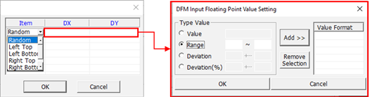
Figure 10. 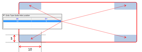
- Ellipse Guide Hole Counting: Verify the number of ellipse type guide
holes at specified regions.
- Clearance between Guide Hole and Components
- Clearance Table: Set and assign a clearance value for the component
group. Use PollEx DFM to verify the
clearance between the component outline and the guide hole edge.
Figure 11. Clearance Table Example 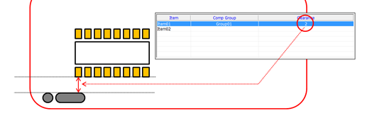
- Remainder: Assign a clearance value for the undefined components in the table.
- Clearance Table: Set and assign a clearance value for the component
group. Use PollEx DFM to verify the
clearance between the component outline and the guide hole edge.
- Checking the location of Guide Hole, matching with Board Origin:
- Guide Hole Selection: Select the target corner of the board.
- Clearance between Guide Hole and Board Outline: Set the clearance value between the guide hole and the selected board corner.
- Clearance Checking:
- Include Checking for Center Guide Holes: Verify the inclusion of the center guide hole selected in the Center Guide Hole Checking is necessary.
- Clearance to Route Pattern: Verify the clearance between the guide hole and route pattern.