Missing Hole
Often, Missing Hole is also referred to as Cutting Region.
For the missing holes, you may have different specifications depending on the
manufacturing processes. The Missing Hole dialog contains the
following sections:
- Missing Hole Definition: Define missing holes in the design using different
methods.
- Component Group: If a missing hole is defined with a component, set
the predefined component group.
- Recognize Missing Hole area on user defined layer: Recognize the area drawn on a specific layer as a missing hole area.
- Missing Hole Via: If vias are used as a missing hole, select them from used via list.
- Figure Missing Hole: If figure hole is used as missing hole, define it with hole size and distance from board outline.
- Component Group: If a missing hole is defined with a component, set
the predefined component group.
- Option: To measure the distance from the missing hole, set the measuring
option.
- Center of Missing Hole: Measure the distance from the missing hole center.
- Edge of Missing Hole: Measure the distance from the edge of the
missing hole area on a certain layer. To define the missing hole
base layer, select layer from layer list.
Figure 1. 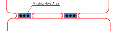
- Checking: Set checking for the various items related to the missing hole in
the PCB.
- Copper (Polygon) Existence Checking in Missing Hole Region: If the missing hole is constructed, copper-pour should be stuffed around the missing hole. If there is no copper-pour, use PollEx DFM to define them as fail.
- Overlapping Check: Check the overlapping with other geometries on
the PCB.
- Board Outline: Check the overlapping with the board outline and the missing hole.
- Silkscreen: Check the overlapping with silkscreen and the
missing hole.
- Set Silk Text Line’s Width as 0.0: While missing hole overlapping check with silkscreen, set the silkscreen text width to zero. To check overlapping with objects, use distance measuring. Zero width for silkscreen text means that distance from the text will be started from the center of text composing line.
- Clearance: Check clearances from various objects.
- Component Clearance: After specifying the component group,
set the clearance between missing hole and components in
group.
- Item: Specify the item name.
- Comp Group: Select the target component group from list.
- Clearance: Set the clearance value between specifying components and missing hole edge.
- Placement: Select the target component placed layer.
- Measure Base: Set the target component measurement base.
- Axis Only: If this option is enabled, PollEx DFM defines fail components
in the region along the missing hole placement
opposite axis.
Figure 2. 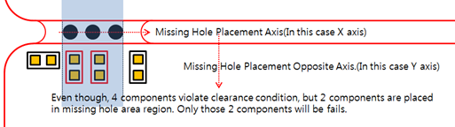
- To PCB Outline: Set the clearance value between the missing
hole and the board outline center.
Figure 3. 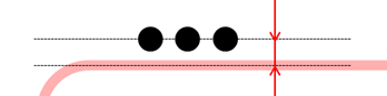
- To PCB Outline’s Rounding Edges: Set the clearance value
between the missing hole and the board outline rounding
edge.
Figure 4. 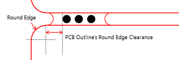
- To Pattern: Set the clearance between the missing hole and
routing patterns.
- Except Copper: While checking the clearance to pattern, except patterns, composing with copper-pour.
- Component Clearance: After specifying the component group,
set the clearance between missing hole and components in
group.
- Hole Pairing: Set rules for the missing hole pair (group).
- Distance of Holes for Group Definition: Set the maximum distance values for grouping missing hole groups. If two missing holes are further apart than the given distance, they cannot be grouped.
- Pair Hole Count: Check the number of missing hole groups.
- Pair Hole Pitch: Set the clearance between the missing
holes.
Figure 5. 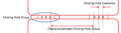
- Missing Hole Group Clearance
- Distance between Missing Hole Groups: Set the clearance between the missing hole groups.
- Distance between Missing Hole Groups and Array Board: Set the clearance value for the missing hole group and the array board.