Ground Wall
Check the clearance for an area affected by ground wall.
Ground walls are design geometries to be used to determine equipment’s movement and
mechanical structure connection with PCB.
- Ground Wall Layer Definition: Define the ground wall.
- Ground Wall Layer for Top: Select the ground wall top layer from the layer list.
- Ground Wall Layer for Bottom: Select the ground wall bottom layer from the layer list.
- Exclude DIP Pin connected Objects: Exclude objects which are connected to the DIP type component pin from target ground walls.
- Exclude Metal Mask Overlapped Objects: Exclude objects which overlap with metal mask from target ground wall.
- Include All Objects in given Layer (Line, Arc, Polyline, and Polygon): Target ground wall object would be all objects on the selected layer. If this option is not checked, target ground wall objects are only objects, drawn with polygon.
- Checking
- Clearance between Ground Wall and Component: Check the clearance
between ground wall and components.
Figure 1. Clearance between Ground Wall Corner and Components 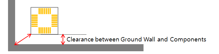
- Item: Specify the item name.
- Comp Group: Select target clearance checking target component from component group list.
- Measure Base: Set target component measurement base.
- Comp Clearance: Set the clearance value between ground wall and specified components.
- Component Clearance at Reverse Side: Set the target component placed.
- Ground Wall Corner: Set the clearance value between components and a ground wall corner.
- Remainder: Check the clearance between ground wall and not
specified components in table.
- Component Clearance: Set the clearance value between ground wall and remaining components.
- Component Measure Base: Set remaining component measurement base.
- Component Clearance at Reverse Side: Set the clearance distance for the remaining components placed on the opposite side of the Ground Wall.
- Clearance between Ground Wall Corner and Remainder Component: Set the clearance value between the ground wall Corner and the remaining components.
- Void-Checking Component Group: Set void-checking components among specifying components in table.
- Exclude Checking for SMD Pins, not having Metal Mask: Define
additional void-checking component SMD pins.
Figure 2. 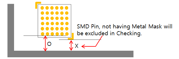
- Clearance between Ground Wall and Solder Mask: Check the clearance
between Ground Wall and Solder Mask.
- Except Component Group: Option to exclude a component group from the checking.
- Except Pad: Option to exclude a Padstack from the checking
using string filter.
- Import(.txt): Apply Filter Type based on the
characters entered in the .txt file.
- Apply as a prefix when (|F|) ABC is entered in the .txt file.
- Apply as a mid-string when ABC is entered in the .txt file.
- Apply as a suffix when ABC(|P|) is entered in the .txt file.
- Export(.txt): Export the characters registered in the String Item in .txt file format.
- Import(.txt): Apply Filter Type based on the
characters entered in the .txt file.
- Clearance between Ground Wall and Vias: Check the clearance between
the ground wall and vias.
- Clearance: Set the clearance value between the ground wall and vias.
- Exclude Blind Via: Option to exclude blind vias.
- Exclude Buried Via: Option to exclude buried vias.
- Exclude Via on Ground: Option to exclude vias that are
connected to Ground Net.
- Net Name: Select ground net from net list.
- Net Name Filters: Set ground net using string
filter.
- Import(.txt): Apply Filter Type based on the
characters entered in the .txt file.
- Apply as a prefix when (|F|) ABC is entered in the .txt file.
- Apply as a mid-string when ABC is entered in the .txt file.
- Apply as a suffix when ABC(|P|) is entered in the .txt file.
- Export(.txt): Export the characters registered in the String Item in .txt file format.
- Import(.txt): Apply Filter Type based on the
characters entered in the .txt file.
- Clearance between Ground Wall and Routing Pattern: Check the
clearance between ground wall and routing patterns.
- Clearance: Set the clearance value.
- Exclude Ground Net: Option to exclude patterns connected to
ground.
- Import(.txt): Apply Filter Type based on the
characters entered in the .txt file.
- Apply as a prefix when (|F|) ABC is entered in the .txt file.
- Apply as a mid-string when ABC is entered in the .txt file.
- Apply as a suffix when ABC(|P|) is entered in the .txt file.
- Export(.txt): Export the characters registered in the String Item in .txt file format.
- Import(.txt): Apply Filter Type based on the
characters entered in the .txt file.
- Clearance between Ground Wall and Component: Check the clearance
between ground wall and components.