Test Point
Verify if the clearance between test points and other objects follow specifications and if the test points contain text.
Detect nets that do not have test points or other objects.
More detailed information:
- Test Point Definition
- Test Point Component Group: Select a test point component group when the test point is drawn as a component.
- Pad Test Point in Route: Recognize test points designed as pads.
- Size: Specify the pad size of the test point.
- Padstack: Select the pad that will be used as a test point by using string filter.
- Via Test Point: Recognize test points designed as a via.
- Size: Specify the pad size of the test point.
- Recognize Plated Through Hole as Test Point: Recognize a plated through hole to the test point.
- Check Net
- All Net: Analyze all nets.
- Selected Net: Select a net for analysis.
- Net Define File: Select a net definition file. The contents of the
file are shown below:
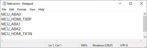
Figure 1. Net Definition File Contents - Jumper Component: Select a jumper component and verify the existence of a test point at both pins of the jumper component.
- Component Connected Nets: Verify the existence of a test point for the net that is connected to the specified component.
- Include Summary of Test Point Placement rate in Excel result report: Display the summary of the test point placement rate in the DFM Result dialog and in the exported Excel sheet.
- Checking
- Component Overlap: Verify if the test point and the components are
overlapped.
- SMD: Verify if SMD components are overlapped with the test point.
- DIP: Verify if through hole components are overlapped with the test point.
- Check Area: Select a measurement base.
- Maximum number of Test Point for each net: Analyze the number of test points for each net and detect if the number is greater than the input value.
- Test Point Clearance <: Analyze the clearance from the test point to another component. The base measurement for the other component will follow the classification settings. If the result is less than the input value, it is detected.
- Test Point Size: Verify the size of the test point and detect if the size of the test point does not match with the specified size.
- Test Point distance from component: Analyze the distance between the
test point and other components connected to the net. If the result
is greater than the input value, it is detected.
- Component Group: Select the component group for analysis.
- Distance <: Enter the distance that the test point should be from a specified component group.
- Unconnected Test Point: Detect if the specified test point objects are not used in the route net.
- Component Overlap: Verify if the test point and the components are
overlapped.
- All Spacing Check Option
- Measure Base
- Test Point: Set a measurement base for the test point.
- Shape: Select a measurement based on the pad shape of the test point.
- Location: Select a measurement based on the center of the test point.
- Pad: Set a measurement base for the pad.
- Shape: Select a measurement based on the pad shape of the pad.
- Location: Select a measurement based on the center of the pad.
- Via: Set a measurement base for the via.
- Shape: Select a measurement based on the via shape of the via.
- Location: Select a measurement based on the center of the via.
- PCB Outline: Set a measurement base for the pcb outline.
- Edge: Select a measurement based on the edge of the pcb outline width.
- Center: Select a measurement based on the center of the pcb outline width.
- Test Point: Set a measurement base for the test point.
- Clearance to Test Point: Analyze the clearance between the test point. If the result is less than the input value, it is detected.
- Clearance to Pad: Analyze the clearance from the test point to the pad of another component. If the result is less than the input value, it is detected.
- Clearance to Via: Analyze the clearance from the test point to the via. If the result is less than the input value, it is detected.
- Clearance to Hole: Use this option to analyze the clearance from the
test point to the hole. If the result is less than the input value,
it will be detected.
- PTH
- NPTH
- Slot PTH
- Slot NPTH
- In the case of slot hole, if the width and height of the hole are different, it is classified as a slot hole.
- Clearance to PCB Outline: Analyze the clearance from the test point
to the PCB outline. If the result is less than the input value, it
is detected.
- Except area from: Exclude analysis if the test point is placed on a specific component area.
- Test Point Zigzag: Detect when the test point is arranged in a series.
- Measure Base
- Existence Checking
- Teardrop: Verify if the test point is assigned the Teardrop shape.
- Test Point on center of Route Pattern: Verify if the test point is not placed in the center of the connected pattern.
- Test Point at the end of Route Pattern: Verify if the test point is
not placed at end of the connected pattern.
- Exclude checking if Route Pattern width is greater than Test
Point: If the route pattern width is wider than a test
point, the test point does not have to be placed at the end
of the connected pattern.
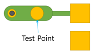
Figure 2. - Exclude checking if the center points between Route Pattern
width and Test Point are different: If the center point of a
test point is not located within a center of route pattern,
the test point does not have to be placed at the end of the
connected pattern.
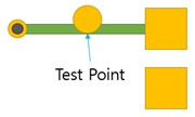
Figure 3.
- Exclude checking if Route Pattern width is greater than Test
Point: If the route pattern width is wider than a test
point, the test point does not have to be placed at the end
of the connected pattern.
- Test Point on Copper Pour: Verify if the test point is placed on the
copper-pour.
- Select Net: Select a net from the list.
- Check Co-Existence Metal Mask and Solder Mask on Test Point: Verify if a metal mask and a solder mask exist within the test point.
- Net Name and TP assigned Text Match Check: Verify the existence of the test
point if the net name contains the specified input string.
- Add Item: Add an item to the table.
- Check Item: Specify the item name.
- Net Name: Specify the net name.
- Solder Mask Checking
- Detect TP un-covered with Solder Mask: Detect a test point without a solder mask.
- Detect TP covered with Solder Mask: Detect a test point with a
solder mask.
- Detect TP un-covered with Solder Mask, when it placed Special Component on the PCB: Detect a test point without a solder mask if a specific component is placed on the PCB.
- Detect TP un-covered with Solder Mask, when TP has a specific Reference Name: Detect a test point without a solder mask if a specific component is connected to the net.