PCB Mark
Recognize a single board by machinery and check the rules about PCB marks.
The PCB Mark dialog contains the following
sections:
- PCB Mark definition: Define the PCB marks in the design.
- Component Group Selection: If the PCB mark is designed with a
component, specify the component group.
- Mask(S/R) Size (SS): Set the PCB mark with the outer mask size.
- PAD Size (PS): Set the PCB mark with the inner pad size.
- Recognize conductive figure shape as Pad: Recognize an object that is drawn with the figure shape in the conductive layer as a Pad.
- Board Figure Geometries: If the PCB mark is defined with board
figure geometries, specify the size of the pad and mask sizes.
- Mask1(S/R) Size (SS): Set the PCB mark with the outer mask size.
- PAD1 Size (PS): Set the PCB mark with the inner pad size.
- Mask2(S/R) Size (SS): Set the PCB mark with the outer mask size.
- PAD2 Size (SS): Set the PCB mark with the inner pad
size.
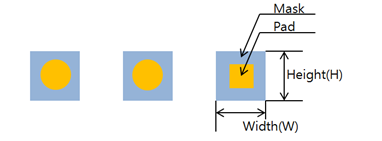
Figure 1.
- Component Group Selection: If the PCB mark is designed with a
component, specify the component group.
- Except checking PCB Mark:
- Major Axis Length <: Exclude the PCB Mark when the PCB major axis is shorter than the setting value.
- Checking
- Copper Existence Check: Use PollEx DFM to
check copper-pours at the same region of the PCB mark. On the same
layer, copper-pour cannot be overlapped with the PCB mark, but on
other layers, there should be copper-pour around the PCB mark.
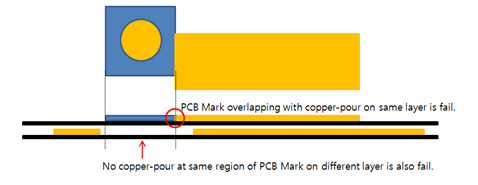
Figure 2. - Placement: Check the placement status of the PCB mark.
- PCB Mark Placed Side(s): Select the layer and use PollEx DFM to check the PCB mark.
- Count: Count the maximum, minimum, or exact number of PCB Marks in the design.
- Exceptional PCB Mark Component: Set the void-checking component group.
- PCB Mark Placed Side(s): Select the layer and use PollEx DFM to check the PCB mark.
- PCB Mark Existence:
- Normal Checking:
- Number of PCB Region: Give the number of regions to divide the PCB.
- PCB Mark Existing Region: Set the region where the
PCB mark is located..
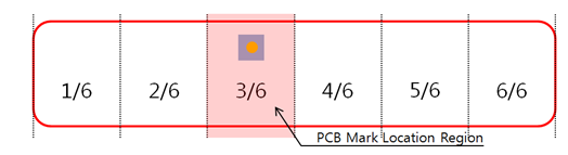
Figure 3.
- Detail Checking:
- The Long Size of PCB: Input the value of a long size range of the PCB.
- Criteria for Count: Select an inequality sign for checking the PCB mark count.
- Minimum Count per Area: Input the minimum number of PCB Marks that should exist in the checking area.
- PCB Mark Existing Region: Set the region where the
PCB Mark is placed.
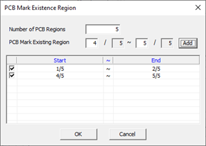
Figure 4. - Number of PCB Region: Set the number of regions to divide the PCB.
- PCB Mark Existing Region: Set the region where the PCB mark is located.
- Normal Checking:
- Silkscreen Overlapping: To check the PCB mark overlap with silkscreen, set comparing GERBER layer for the top and bottom.
- Clearance Checking:
- Component: To check the clearance between the PCB mark and components, set the clearance value.
- Route Patterns: To check the clearance between the PCB mark and route patterns, set the clearance value.
- Copper-pour: To check the clearance between the PCB mark and copper-pour, set the clearance value.
- Via: To check the clearance between the PCB mark and vias, set the clearance value.
- Board Outline: To check the clearance between the PCB mark and the board outline, set the clearance value.
- Copper Existence Check: Use PollEx DFM to
check copper-pours at the same region of the PCB mark. On the same
layer, copper-pour cannot be overlapped with the PCB mark, but on
other layers, there should be copper-pour around the PCB mark.