Wave Mark
Check wave mark in the FPC component edge.
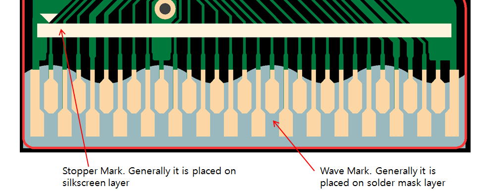
Figure 1.
- Wave Mark Definition: Wave mark is mark for the connector solder mask.
Define wave marks in the design.
- Component Group Selection: Define target components which should have wave mark. Select them from the component group list.
- Wave Mark Layer: Select the layer on which wave mark should be placed. Select the layer from the layer list.
- Stopper Mark Definition: The purpose of stopper mark is mark for stopping
line while connector plugged in. Define stopper marks in the design.
- Component Group Selection: Define target components which should have stopper mark. Select components from the component group list.
- Stopper Mark Layer: Select the layer on which the stopper mark should be placed. Select the layer from the layer list.
- Checking:
- Check Existence of Wave Mark: Check if target components have wave mark on specifying layer.
- Check minimum Pattern’s Width, connected to Wave Mark: Check if the
pattern width has enough thick in certain region.
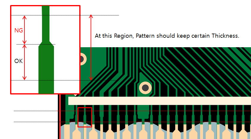
Figure 2.- Keep Pattern’s Width in given Distance from Wave Mark: In
certain region, patterns width should not be changed.
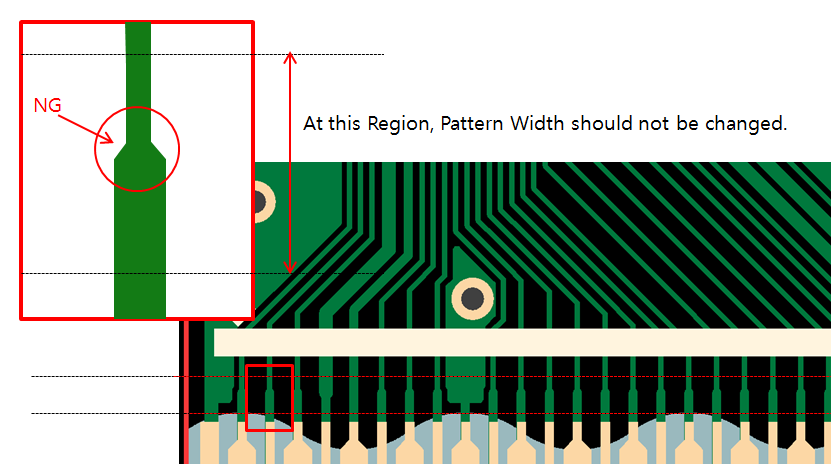
Figure 3.
- Keep Pattern’s Width in given Distance from Wave Mark: In
certain region, patterns width should not be changed.
- Check Existence of Stopper Mark in Distance from Wave Mark: Checks
the stopper mark existence within certain distance from wave
mark.
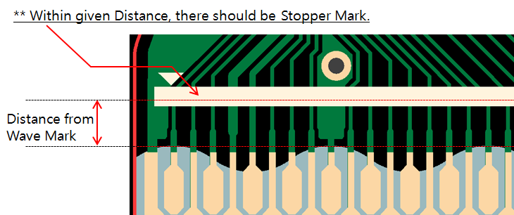
Figure 4.- Distance: Set the searching distance from wave mark.