Via Spacing
Depending on the via type, check different clearance to different PCB objects.
In many cases, if the distance between via and component pads is close, it may result
in lead flow to pads in the soldering process. To keep the distance, a soldering
engineer has to check layout design precisely. Via Spacing checks clearances from
via to component, solder mask, or component pad.
- Laser Via Definition: Define laser via.
- Maximum Hole Size: Define the via with maximum hole size that same and smaller holes will be recognized as a layer via.
- Padstack List: Define the via using padstack name.
- Padstack String: Define the via using string filter.
- Via Boundary Definition: Define the via boundary. Select one of two items
between pad shape and hole shape. This will be used to measure the distance
from other objects to via.
- Via’s outer Pad Shape: Via pad outer shape will be used as via boundary.
- Via’s Hole Shape: Via hole will be used as via boundary.
- Component Definition
- BGA Component Selection: To define target BGA components, select BGA components from the component group list.
- Excluding-Component Selection: Select a component group to exclude from checking.
- Checking
- Zigzag Checking for Via: Finds vias on design and checks if they are
placed in zigzag style. If they are not matching with zigzag style,
PollEx DFM finds that locations and
defines them as fails.
- Select Target Vias in given maximum Distance: Set the
maximum distance value between two vias.
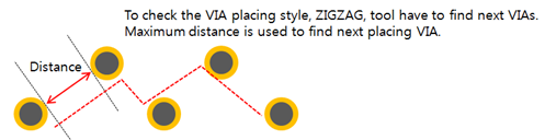
Figure 1. - Shape (Edge to Edge) / Location: To define zigzag style of
via placement, tool should find next via. To do find next
via, tool use distance from base via to another via.
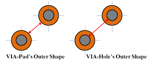
Figure 2. - Check Vias in same Net: In distance checking between via, default is not checking distance between vias in same net. But if this option is checked, PollEx DFM will check for vias in same net.
- Select Target Vias in given maximum Distance: Set the
maximum distance value between two vias.
- Clearance between BGA Component’s Pad and Via: Check minimum
distance between BGA pin pad and other vias.
- Clearance to same Net: Set clearance value between to target the BGA component pad and vias with the same net property.
- Clearance to different Net: Set clearance value between to target the BGA component pad and vias having different net property.
- Clearance between Solder Mask and Via: Check minimum distance
between solder mask and vias.
- Clearance: Set the clearance value between solder mask and vias.
- Exclude Vias, connected to specifying Net: At above checking, exclude vias with certain net property in checking. To define void checking vias, select net from net list.
- Exclude checking for Laser Via: Option to exclude the Laser Via from checking.
- Exclude checking for Solder Mask, Not having Metal Mask: Option to exclude the Solder Mask that does not have the Metal Mask from checking.
- Clearance to Pad: Check the clearance between components’ pad to vias.
- Exclude Via Pad Overlapped on BGA’s Reverse Side: Option to exclude a component placed on the opposite side of BGA component.
- General Clearance to Pad: Set clearance value between component pad and vias.
- Detail: Using this option, you can define different detail
clearances for various types of via. Basically, Via Spacing
item’s checking Detail has clearance checking functions for
Through, Blind, Buried, and Laser Vias. Each of them has
same specification tables. Checking will be done for objects
on same layer as via starting layer or for all layers. To
SMD, DIP component pins and vias, you can assign different
clearance values. Also, in one clearance checking, you can
assign different values for objects in same net and other nets.
- Clearance to SMD Pad: Check the clearance between the selected type of via and SMD pin pad.
- Clearance to DIP Pad: Check clearance between the selected type of via and DIP pin pad.
- Clearance to Via: Check clearance between the selected type of via and other vias.
- Compulsory Use Boundary as Via’s Hole Shape in same Net Checking: For the checking Clearance to via, if this is turn-on, use vias outer Pad Shape option in via Boundary Definition for measuring via to via distance. For above three checking rules, they all can have different clearance for same net and other nets. At checking, users have different detail checking options.
- Exclude Vias overlapping with Solder Mask: Option to exclude vias overlapped with the Solder Mask from checking.
- Except for Pad on Via (Only Same Net): PollEx DFM doesn’t check for vias on SMD pads in case they are having same net property.
- Except for SMD Pins, not having Metal Mask: PollEx DFM doesn’t check for SMD pads which have no metal mask in selected component group. To specify target component, select components from the component group list.
- Except for Overlapped Same Net: If pin and via are directly connected in the same net, checking will be skipped.
- Zigzag Checking for Via: Finds vias on design and checks if they are
placed in zigzag style. If they are not matching with zigzag style,
PollEx DFM finds that locations and
defines them as fails.