Hole Through Pad
Check holes placed on component pads.
- Target Object Definition: Define checking target objects.
- Through Hole Via: Through hole via will be checking target objects.
- Exclude GND connected Via: Among target objects, exclude vias connected to ground net. To specify the ground net, select ground net from net list.
- Exclude Vias with specific Hole Size Ranges: To exclude certain vias from target objects, specify holes’ size ranges.
- Blind Via: Blind vias will be checking target objects.
- Exclude GND connected Via: Among target objects, exclude vias connected to ground net. To specify the ground net, select ground net from net list.
- Exclude Vias with specific Hole Size Ranges: To exclude certain vias from target objects, specify holes’ size ranges.
- Through Hole Via: Through hole via will be checking target objects.
- Checking
- HOLEs on Pad: Check holes are placed on component’s pad.
- Clearance between Hole and Component Pads: Set the clearance
value between target vias’ holes and components.
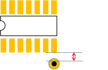
Figure 1. - Via Measure Base: Select the Via measure base.
- Pad Shape: Check based on Via Pad Edge.
- Hole Shape: Check based on Via Hole Edge.
- Component Group: Select target component group.
- Pad Measure Base: Select the Pad measure base.
- Pad: Set a Pad area as a measure base.
- Pad + Solder Mask Overlap: Set a measure base where the Pad and the Solder Mask are overlapped.
- Solder Mask: Set a Solder Mask area as a measure base.
- Excluding Components: Exclude components in checking with selecting component group from list.
- Excluding the specific Pad: Option to exclude the specific
pad from checking.
- The largest area of pin pads: Recognize the largest pad of the component as a target object.
- Larger than average area of pin pads: Recognize the pads larger than the average pad area of the component as a target object.
- The smallest area of pin pads: Recognize the smallest pad of the component as a target object.
- Check for thermal Pads: Check for components’ thermal pads.
Default checking doesn’t check for components’ thermal
pads.
- Except Component: Option to exclude a component from the Thermal Pads checking.
- Via Measure Base in Thermal Pad Area: Define the Via measure base on the Thermal pad and via checking.
- Pad Shape: Set the Pad Shape as a measure base.
- Hole Shape: Set the Via Hole’s Edge as a measure base.
- Via Location: Set the Via center as a measure base.
- Except Via in Pad Area: Option to exclude Vias placed inside
the pad area from checking.
- SMD: Exclude Vias placed inside the SMD pad (When SolderMask is smaller than pad.) area from checking.
- NSMD: Exclude Vias placed inside the NSMD pad (When SolderMask is larger than pad.) area from checking.
- Via Measure Base in Pad Area: Define the Via measure
base on the pad and via checking.
- Pad Shape: Set the Pad Shape as a measure base.
- Hole Shape: Set the Via Hole’s Edge as a measure base.
- Via Location: Set the Via center as a measure base.
- Exclude Checking for SMD Pins, not having Metal Mask: Option to exclude SMD Pins that do not have Metal Mask from checking.
- Clearance between Hole and Component Pads: Set the clearance
value between target vias’ holes and components.
- Check Via Hole Existence within Component Area: Check whether vias
hole are in component boundary.
- Target Component Group: Select target components from component group list.
- Via Location on Pad’s Center: If via placed on pad’s area, they
should be placed at same location. Item checks whether they are at
same location or not. If their locations are different, it is
fail.
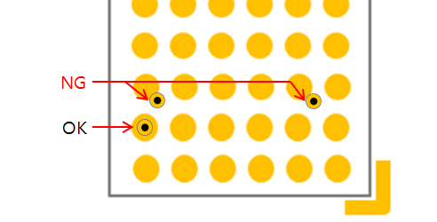
Figure 2.- Item: Specify the item name.
- Comp Group: Select target components from component group list.
- Via Type: Select via type.
- Tolerance: Set tolerance value. Within tolerance, PollEx DFM treats them as same location.
- Via's on Pad's Symmetry: Check whether the via hole is located on the component pad's central axis (long axis).
- Via Stackup: Allowable maximum number of via’s passing physical layers.
- Exclude Checking for SMD Pins, not having Metal Mask: Option to exclude SMD Pins that do not have Metal Mask from checking.
- HOLEs on Pad: Check holes are placed on component’s pad.