Thermal Pad
Check rule for component thermal pads.
Thermal Pad is used to raise thermal conductivity for the purpose of heat
dissipation.
- Checking
- Item: Specify the item name.
- Component Group: Select target components from component group list.
- Exclude Component Group: Select void-checking components among target components by selecting void-checking component group list.
- Checking Option: Upon double-clicking column, the new
optional dialog will appear. In the dialog, set
detail checking options.
- Thermal Pad Definition: Define the criteria to recognize the
Thermal Pad in the component area.
- Pad: Recognize as a Thermal Pad if the Pad is placed inside the component area.
- Copper Polygon: Recognize as a Thermal Pad if the Copper-Pour is filled inside the component area.
- Laser Via Definition: Define the Laser Via.
- Minimum Hole Size: Define the Laser Via with the Hole Size. Vias with the hole size below the entered value are considered as the Laser Via.
- Via PadStack Selection: Select the Laser Via through the Via PadStack list directly.
- Check the Number of Solder Mask and Metal Mask in Thermal
Pad: Check the number of solder / metal masks.
- Size / Area: Selecting searching unit between size and area.
- Item: Specify the item name.
- Pad Size/Pad Area: Depending on target pad searching unit, set the value range of size or area.
- Number of Solder Masks: Set the number of solder masks. If the number of solder masks does not match the given value, it is a fail.
- Number of Metal Masks: Set the number of metal masks. If the number of metal masks does not match the given value, it is a fail.
- Checking Options
- Target Via: Select the target via.
- Through Via: Option to include the Through hole via from checking.
- Blind Via: Option to include the Blind via from checking.
- Buried Via: Option to include the Buried via from checking.
- Laser Via: Option to include the Laser via from checking.
- Via Measure Base: Select measure base for via.
- Hole Shape: Measure based on the edge of the Via Hole Shape.
- Via Pad: Measure based on the edge of the Via Pad shape.
- Via Location: Measure based on the center of the Via Pad shape.
- Check Existence of Thermal Pads in Target Component: Check if target component has thermal pad or not. If it has no thermal pad, PollEx DFM detects it.
- Check Existence of Vias in Metal Mask Region: Check if vias are placed on metal mask in thermal pad. If vias are placed on metal mask region, it is a fail.
- Check Existence of Solder Mask in Via’s region at
reverse Side of Thermal Pad: Check if solder mask is
overlapped with via on reverse side of thermal pad
placed layer. If so, it is a fail.
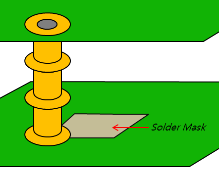
Figure 1. - Check co-Existence of Solder Mask and Metal Mask in Thermal Pad: Check if solder mask and metal mask exist at the same time. If one of them is not in thermal pad, it is a fail.
- Check Size Matching with Solder Mask and Metal Mask in Thermal Pad: Check metal mask and solder mask size. If they are not same in size, it is fail.
- Expand Thermal Pad Area: Set the expanding size value for thermal pad region.
- Check direct Connection between Pin and Thermal Pad: Check if there is a routing pattern connecting thermal pad and pin of component. If there is direct connection, it is a failed.
- Clearance between Via and Via in Thermal Pad: Check clearance between via and via in Thermal Pad area.
- Clearance between Thermal Via and the Component Pads placed on the opposite side of the Thermal Pad.
- Check the Number of Vias in Thermal Pad: Check the
number of vias in thermal pad.
- Number of \Vias: Specify the number of vias. If the result does not match the given number, it is a fail.
- Exclude GND connected Via: If this option is checked, exclude GND connecting vias in counting the number of vias.
- Exclude Vias overlapped with Silkscreen: If this option is checked, exclude silkscreen overlapped vias in counting the number of vias.
- Clearance between Thermal Pad and Via: Check
clearance between thermal pad and vias.
- Clearance: Set the clearance value between thermal pad and vias.
- Exclude GND connected Via: If this option is checked, exclude GND connecting vias in counting the number of vias.
- Do not check in case of Thermal Pad and Via have same Net: If via and thermal pad have same net name, PollEx DFM will not do clearance checking.
- Target Via: Select the target via.
- Thermal Pad Definition: Define the criteria to recognize the
Thermal Pad in the component area.