Copper Connected Pad
Check specified components pattern connected pin area ratio.
If patterns are widely connected to a pin, excess heats transfer to pins and result in cold solder in soldering process. To prevent this unpredictable malfunction, small ratio of connection area is need.
Checking: Check ratio of connected patterns width against the around length pins.
- Checking: Check the ratio of connected patterns’ width against the around
length of pins.
- Item: Specify the item name.
- Component Group: Select target components from component group list.
- Checking Type: Select one of the two checking types below.
- Connected copper width ratio: Checking the ratio of the total connected copper length to the total pad’s perimeter length.
- Exposed Copper area ratio: Checking the ratio of exposed copper in the area between the pad and the solder mask.
- Tie leg quantity: Checking the quantity of tie leg.
- Tie leg width: Checking the width of tie leg.
- Tie leg length: Checking the length of tie leg.
-
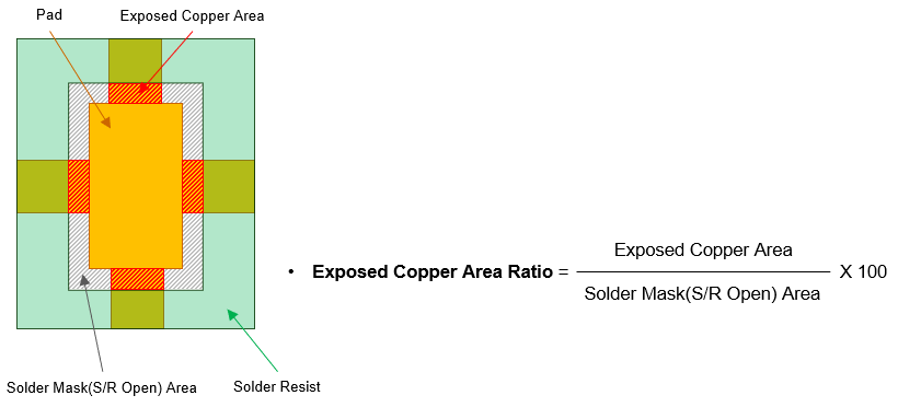
Figure 1.
- Filter: Set the ratio condition of pattern and copper-pour where
connected to the target pad.
- >=: If the check result of the Pattern/Pad ratio is greater than or equal to the input value in Pattern Width, it is passed. If the result is less than the Pattern Width value, it is failed.
- <=: If the check result of the Pattern/Pad ratio is less than or equal to the input value in Pattern Width, it is passed. If the result is greater than the Pattern Width value, it is failed.
- >: If the check result of the Pattern/Pad ratio is greater than the input value in Pattern Width, it is passed. If the result is less than or equal to the Pattern Width value, it is failed.
- <: If the check result is less than the input value in Pattern Width, it is passed. If the result is greater than or equal to the Pattern Width value, it is failed.
- =: If the check result of the Pattern/Pad ratio is equal to the input value in Pattern Width, it is passed. If the result is not equal to the Pattern Width value, it is failed.
- Ratio(%): Select the maximum ratio of connected patterns width against pin’s surrounding length.
- Except Thermal Pad: Among pads in target components, except checking for thermal pads.
- Filter Type: To select target components’ checking pads, users can use net name or pin name.
- Pin/Net Name Filter: Upon double-clicking the column, add the keyword for pin name or net name for selecting pads.
- Small Area Size: Set pad connected copper area’s dimension. If
connected copper’s dimension is small than given value, even though
checking result is fail, PollEx DFM define it as passed. It means
small pin connected copper prevent cold soldering in cooling
process.
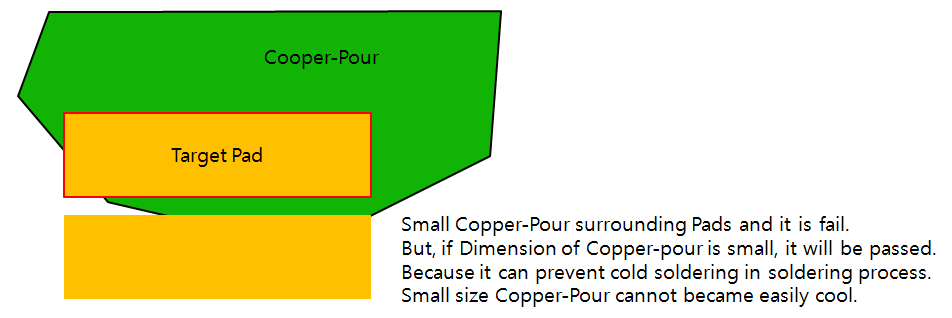
Figure 2. - Based on Specific Pad: Option to define a Pad as a target which
meets the specific condition.
- The largest area of pin pads: Recognize the largest pad of the component as a target object.
- Larger than average area of pin pads: Recognize the pads larger than the average pad area of the component as a target object.
- The smallest area of pin pads: Recognize the smallest pad of the component as a target object.