Via Spacing 2
Check via clearance depending on via size.
- Via Class Definition: Define the via information such as type, hole size,
and measurement base with clearance value. It is possible to add the via
class on the list by clicking Add Via Class.
- Via Class Name: Specify the Via Class name.
- Via Type: Define the type among All, Through Via, Blind Via, Buried Via, Via Padstack, and Via String Filter. Via type will be detected automatically following PCB design information.
- Hole Size: Define via hole size such as certain value or range.
- Via Padstack: In case of via Padstack, it can select via from the padstack list dialog if you choose this. (Click the Hole Size menu to be enable this.)
- Measure Base: Select one of two items between pad shape and hole
shape. This will be used to measure the clearance from other objects
to via.
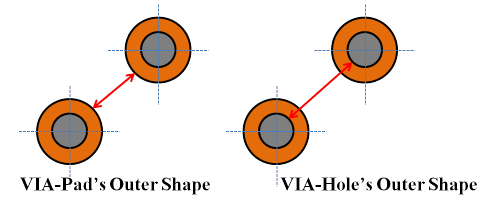
Figure 1.- Pad Shape: Via pad outer shape will be used as via boundary.
- Hole Shape: Via hole will be used as via boundary.
- Clearance to Via: To check the clearance between via to via. Each
combination will be generated automatically by clicking Default
Reset. Clearance value will be defined by getting Via Class
Definition, and you can change or define the measure base with each
clearance value.
- Keep Other Values while Adding new Classes Combination: To keep the previous setting when adding a new via Class, select this option.
- Clearance to PAD: To check the clearance between via to PAD of component. Select Component Group and then select Via Class. Measure base can be defined here with clearance value depend on target net such as SMD (Same Net), SMD (Other Net) and DIP (Same Net), DIP (Other Net).