Teardrop
Check rule related to teardrop in design.
Teardrop is used to avoid a pocket (where the trace meets the pad) that could collect
acid from the PCB etching process which would later do bad things. Also, it reduces
mechanical and thermal stress resulting in less hairline cracks in the
trace.
- Target Objects Definition: Define target pin type or vias.
- SMD Pad: Target objects will be SMD type pads.
- DIP Pad: Target objects will be DIP type pads.
- Via: Target objects will be vias.
- All: Target objects will be All vias.
- Hole Size: Set the hole size of the via to define the target
objects.
- Annular Ring Size: Set the annular ring size for the vias that meet the hole size criteria.
- Target Components Definition: Define target components.
- All Components: All components will be target components.
- Component Group Selection: Select target components by selecting component group from list.
- Checking
- Find Different Pad Shape in Component: Find different padstacks than
specifying padstack.
Figure 1. 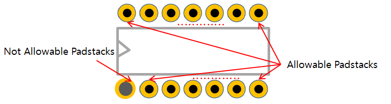
- Target Component: Select target components from the component group list.
- Padstack Name Filter: To specify allowable padstack, define allowable padstack name with name combination. Use name filter, defining padstack name starting with, ending with or include strings.
- Teardrop Existence: Check the teardrop existence on pad or vias.
- Exclude Checking for following Condition: Exclude checking
for following conditions pads or vias.
- Connecting thick Patterns than Pad Size: If the pattern width is thicker than pad size, it is not checking target.
- Ignore for Via/Pin with Thermal: Option to exclude from checking the Through Hole Pin and Via that applied the Thermal relief.
- Connecting thick Patterns than given Value: If the pattern width is thicker than given value, it is not checking target. Set the pattern’s width value.
- Vias on Pad: If a via is placed on pad, it is not checking target.
- Accept multiple connected Patterns as Teardrop for much more
than given Number: If multiple patterns are connected to pad
or via, PollEx DFM checks the
number of connected patterns and if they are many more than
given number, it is fail.
Figure 2. 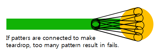
- Minimum length of Teardrop: Check the teardrop length.
- Pad Measure Base: Set the Pad Measure Base to Edge or Center.
- SMD Pad: Set the minimum length of SMD Pad's Teardrop.
- DIP(PTH) Pad: Set the minimum length of DIP(PTH) Pad's Teardrop.
- Via Pad: Set the minimum length of Via Pad's Teardrop.
- Exclude Checking for following Condition: Exclude checking
for following conditions pads or vias.
- Find Different Pad Shape in Component: Find different padstacks than
specifying padstack.