Solder Resist Pad
Solder Resistor (SR) is a material which is applied to specific areas of the printed circuit board during a soldering process and protects the circuit of the unnecessary portions of solder.
- Solder Mask Layer Definition
- Top: Define the Solder Mask layer of the Top layer.
- Bottom: Define the Solder Mask layer of the Bottom layer.
- Checking
- Item Name: Specify the item name.
- Component Group: Select target components with component group selection.
- Check Options: Upon double-clicking column, Check Options,
run checking option dialog as below.
Figure 1. 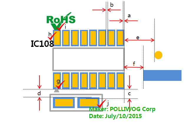
- Merge Overlapped Solder Masks: If the solder mask overlaps,
merge it into one for inspection (Merge is applied only when
they are part of the same component).
- Comp Pad & Comp Pad: Merge the solder masks of the component pads.
- Comp Pad & Comp Figure: Merge the solder mask of the component pad with the solder mask of the component figure.
- Comp Pad & Board Figure: Merge the solder mask of the component pad with the solder mask of the board figure.
- Comp Figure & Comp Figure: Merge the solder mask of the component figure.
- Comp Figure & Board Figure: Merge the solder mask of the component figure with the solder mask of the board figure.
- Board Figure & Board Figure: Merge the solder mask of the board figure.
- Clearance between Solder Mask and Pad in Same Component: Set
the clearance value between solder mask and pad.
- SMD: Set the clearance value between solder mask and SMD pad.
- NSMD: Set the clearance value between solder mask and NSMD pad.
- Maximum distance between Solder Mask and Pad in same
Component: Even if the distance between the pad and
solder mask satisfies the upper inspection option
Clearance condition, if it exceeds the maximum
distance value Fail.
- SMD: Set the clearance value between solder
mask and SMD pad.
- If the Solder Mask is entirely within the Pad area, it is considered an SMD Pad.
- NSMD: Set the clearance value between solder
mask and NSMD pad.
- If the Pad is entirely within the Solder Mask area (including cases where they are the same size), it is considered an NSMD Pad.
Figure 2. 
- SMD: Set the clearance value between solder
mask and SMD pad.
- Regard Pad as Pass with having greater than given value for any direction: On the clearance checking between the edges of Pad and Solder Mask, this option is considered to pass if either direction is satisfied.
- Except for Other(Not in SMD or NSMD)Pad Type: Exclude Other Pad Type from the fail result.
- Clearance between Solder Masks in Same Component: Set the clearance value between solder mask and solder mask.
- Clearance between Pad and Other Component’s Solder Mask: Set the clearance value between pad and other components’ solder masks.
- Clearance between Solder Mask and Other Component’s Solder Mask: Set the clearance value between solder mask and other component solder masks.
- Clearance between Solder Mask and Board Figure Pads: Set the clearance value for solder mask and board figure type pads.
- Clearance between Solder Mask and Board Figure Solder Masks: Clearance checking between the Solder Masks of Pad and Board Figure.
- Clearance between Solder Mask and other Net: Clearance
checking between the Solder Masks of Pad and Net.
-
Except for the figure solder masks which remove the solder mask dam between the pads: If a component's pad is covered by Board Figure S/M or Comp Figure S/M, it is considered a pass if the pattern shape is in contact with the pad shape.Note: Apply only when the pattern is directly connected to the pin.
-
Recognize as different nets if other nets are connected to the same reference.
-
- Check exposed copper on the same net due to solder mask.
- Solder Mask Overlapping with Component Figure Silkscreen: Option to check the area where the Solder Mask and Component Figure silkscreen overlap. Overlapped area is considered as fail.
- Solder Mask Overlapping with Component Text Silkscreen: Option to check the area where the Solder Mask and Component Text silkscreen overlap. Overlapped area is considered as fail.
- Solder Mask Overlapping with Board Figure Silkscreen: Option to check the area where the Solder Mask and Board Figure silkscreen overlap. Overlapped area is considered as fail.
- Solder Mask Overlapping with Board Figure Text Silkscreen: Option to check the area where the Solder Mask and Board Figure Text silkscreen overlap. Overlapped area is considered as fail.
- Check Existence of Solder Mask in Target Component’s Pin: Check whether target component’s pin has solder mask or not.
- Check the existence of Solder Mask between Thermal Pad and I/O Pad: Check whether Solder Mask exists between Thermal Pad and I/O Pad.
- Solder Mask Usage
- Check Solder Mask usage in multiple Pins: Check multiple
shares same solder mask.
Figure 3. 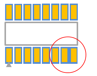
- Check Solder Mask usage between Pins(Only 2Pin Component): Option to check whether the Solder Mask is filled between the Pads where the component has only 2 pins.
- Check Solder Mask Covered on Component Area: Option to check whether the component area is covered with the Solder Mask.
- Measure Base: Select measure base.
- Expand Component Boundary: Enter the value to be expanded the component boundary area.
- Merge Overlapped Solder Masks: If the solder mask overlaps,
merge it into one for inspection (Merge is applied only when
they are part of the same component).
- Remainder: Check above same rules for components which are not listed in table.
- Display Fail Results for Each Pin: Display the fail results for each pin of the component.
- Board Figure Solder Mask: Checking rules for solder masks belong to board
figure.
- Clearance between Board Figure Solder Mask: Set the clearance value
between board figure solder masks and others.
- Including Board Figure having Pad: Option to include the Solder Mask of Board Figure having Pad.
- Overlapping with below Types of Silkscreen: Check silkscreen data’s
overlapping with board figure geometries.
Figure 4. 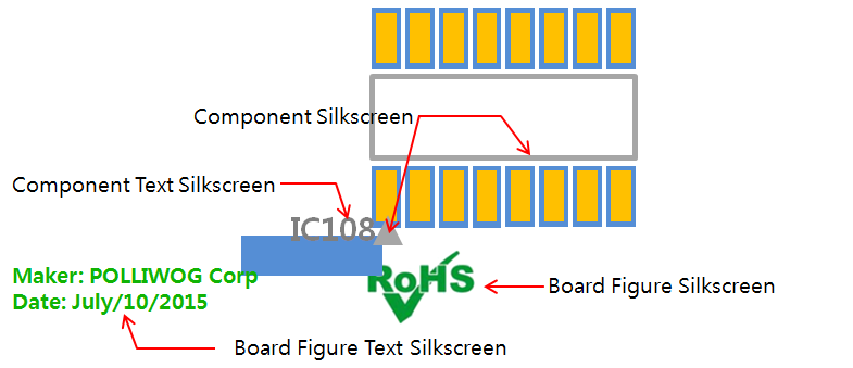
- Component Figure: Option to check whether the Solder Mask and Component Figure silkscreen overlap.
- Component Text: Option to check whether the Solder Mask and Component Text overlap.
- Board Figure: Option to check whether the Solder Mask and Board Figure silkscreen. overlap.
- Board Figure Text: Option to check whether the Solder Mask and Board Figure Text silkscreen overlap.
- Clearance between Board Figure Solder Mask: Set the clearance value
between board figure solder masks and others.