Silk Print Between Two pins
Check the existence of silkscreen between two pins of DIP type components.
In the wave-soldering process, silkscreen between two pins is necessary to prevent solder flow from one to another.
The Silk Print Between Two Pins dialog contains the following
sections:
- Target Components Definition
- Component Group Selection: Component selection when selecting from the group list.
- Selection by Pin Pitch: Among the selected component group, target
components will match with the following conditions.
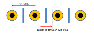
Figure 1.- Condition: Select And or Or condition for the Pin Pitch option that is entered in 2) ~ 4).
- Maximum Pin Pitch (Center to Center): Target components will be the component that has smaller pin pitches.
- Minimum Pin Pitch (Center to Center): Target components will be the component that has larger pin pitches.
- Maximum Distance between Pin Edges: Target components will be the component that has a smaller distance between two pin edges.
- Minimum Distance between Pin Edges: Target components will be the component that has a larger distance between two pin edges.
- Silkscreen Layer Definition
- Silkscreen Layer Selection: Select the silkscreen layer from the layer list.
- Target Layer Definition: Select the layer where the silkscreen should be
placed.
- Component Placed Layer: If the component is placed on top, silkscreen should be placed on the silkscreen top layer. Vice versa is also valid.
- Opposite Side of Component Placed Layer: If the component is placed on top, silkscreen should be placed on bottom layer and vice versa.
- Both: Top and bottom silkscreen will be passed.
- Option
- Display Fail Result for All Pins. (Default: Display representative
One Fail for a Component): PollEx DFM shows
a representative a fail result for the components fail. Using this
option, keep all fail occurring points in the result.
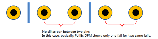
Figure 2.
- Display Fail Result for All Pins. (Default: Display representative
One Fail for a Component): PollEx DFM shows
a representative a fail result for the components fail. Using this
option, keep all fail occurring points in the result.