First Pin Mark
Check the existence of the components first pin mark and overlapping with other objects.
Generally, the components first pin mark is designed with silkscreen. You can use a different type of first pin mark.
The First Pin Mark dialog contains the following
sections:
- Target Component Definition
- Component Group: Select the target component from the group list.
- Exclude Checking for Components which do not have Mark: After searching the first pin mark for specified component group, if PollEx DFM fails to find first pin mark, PollEx DFM will skip checking for those components.
- First Pin Mark Layer Definition: To get the first mark, define the
top and bottom layer where the first pin mark should be designed.
- Top Mark Layer: Select the top first pin mark layer.
- Bottom Mark Layer: Select the bottom first pin mark layer.
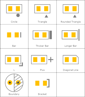
- First Pin Mark Shape Definition: Select the shape of the First Pin
Mark.
Allowable polarity mark types in PollEx DFM are as follows: If the following types of polarity marks are detected in the searching area, PollEx DFM recognizes that the component has a polarity mark.
Figure 1. 
- First Pin Mark Checking
- Check First Pin Mark with Character String: Upon selecting this option, PollEx DFM searches the first pin mark with a given character string near the first pin mark.
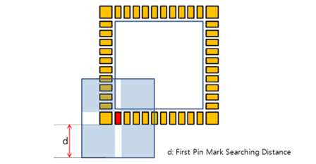
- Check First Pin Mark within First Pin Area for Board Figure
Geometry: If first pin mark is designed with board figure geometry,
PollEx DFM searches for the first pin
mark within the area near first pin.
- Searching Distance from First Pin: Set the distance from the
first pin.
Figure 2. 
- Searching Distance from First Pin: Set the distance from the
first pin.
- First Pin Mark Overlapping Check
- Overlapping with Silkscreen: Check if the first pin mark is overlapping with another silkscreen.
- Overlapping with Pad: Check if the first pin mark is overlapping with another component pad.
- Overlapping with Via Hole: Check if the first pin mark is overlapping with the via hole.
- Overlapping with Board Figure Hole: Check if the first pin mark is overlapping with the board figure hole.