Pad Size by Pin Pitch
Check the pad size depending on the pin pitch for fine pin pitch components.
The Pad Size by Pin Pitch dialog contains the following
sections:
- FPCB Layer Definition: In the case of Rigid-Flex PCB, Rigid PCB is stacked
based on the FPCB layer. Set up the FPCB layer to distinguish between the
FPCB and Rigid PCB layer.
- FPCB Layer Filter: Set FPCB layer using String Filter
- Layer Name: Recognize the FPCB Layer based on the Layer Name.
- Layer Comment: Recognize the FPCB Layer based on the Layer Comment.
- User Defined Layer: Select the layer that FPCB area is drawn from the layer list.
- FPCB Layer Filter: Set FPCB layer using String Filter
- Pad Size and Pin Pitch Checking: Check components pin pitch and pad
size.
- Item: Specify the item name.
- Component Group: Double-click the column and select the component group from the group list dialog.
- Layer: Specify the target layer.
- Pin Pitch: Set the pin pitch using the floating value ranges input tool.
- FPCB Area: Option to check the Pad Size in the FPCB area.
- Pad Width: Set the pad width using floating value ranges input tool.
- Pad Height: Set the pad height using floating value ranges input tool.
- Solder Mask Width: Set the solder mask width using floating value ranges input tool.
- Solder Mask Height: Set the solder mask height using floating value ranges input tool.
- Metal Mask Width: Set the metal mask width using floating value ranges input tool.
- Metal Mask Height: Set the metal mask height using floating value
ranges input tool.
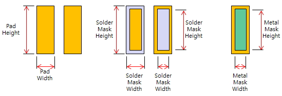
Figure 1.