Edge Pin Size
Check the edge pin size ratio to common pins.
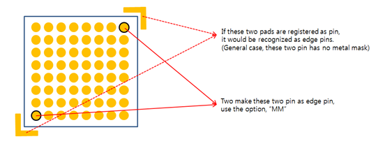
BGA or CSP type packages are very weak in the soldering process. To overcome this weakness, designers should do some special designs for the edge pins in these packages. Normally, edge pin size should be bigger than a common pin size.
- Edge Pin Size Checking: Check the ratio of edge pin size to common pin
size.
- Item: Specify item name.
- Component Group: Upon double-clicking the Component Group column, the component group list dialog opens. Select target component group from list.
- Pass Condition: It means size ratio of edge pin to common pin should be bigger (>), equal (=) or smaller (<). Set the conditions.
- Ratio: Set edge pin size ratio against common pin.
- MM: To avoid PollEx DFM recognizing the
wrong edge pin, use this option so that PollEx DFM will not treat pins that have no
metal mask as edge pins.

Figure 1. - Copper Existence: Checks whether copper exists between the edge pad
and the exposed (thermal) pad. If Copper Polygon or Route Pattern
exists in the designated area and Solder Mask does not exist, it is
Pass, If Solder Mask exists in the designated area, it is Fail.
- Component Group: Select target component group from list.
- Check copper existence on the inner side of the row end pads: Set the clearance for copper and inner side of the row end pads.
- Check Solder Mask existence on the inner side of the row end pads: Set the clearance for Solder Mask and inner side of the row end pads.