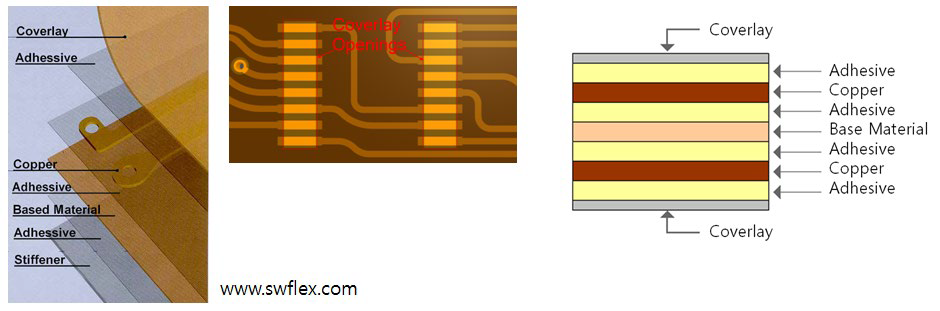
The Coverlay is the insulating layer placed over the exposed conductors. It is
typically constructed of a pre-cut piece of polyimide film laminated over the
conductors using either acrylic or epoxy adhesive. Coverlay is used to protect and
insulate the exposed surface of the circuit. Figure 1. Figure 2.
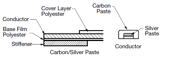
Screen printing with conductive ink is the newest form of FPC (called membrane) being
produced today. In this application, carbon/silver (C/Ag) paste replaces the
traditional copper conductor. Figure 3.
The Coverlay dialog
contains the following sections:
Layers Definition: Define target layer for checking.
Coverlay Top Layer: Select the top Coverlay layer from layer
list.
Coverlay Bottom Layer: Select the bottom Coverlay layer from layer
list.
Silver Paste Top Layer: Select the top silver paste layer from layer
list.
Silver Paste Bottom Layer: Select the bottom silver paste layer from
layer list.
Checking
Clearance between Coverlays: Check the clearance between Coverlay
and Coverlay on the same layer.
Minimum Coverlay Size: Check Coverlay size. If the width or height
of a Coverlay is smaller than given value, it is a fail.
Width: Set the width value for single a Coverlay.
Height: Set the height value for single a Coverlay.
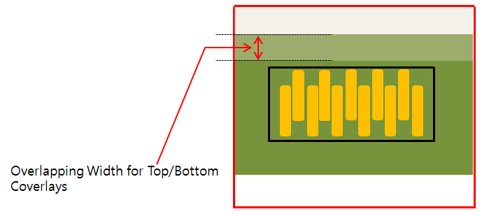
Check Overlapping Width between Top and Bottom Coverlay: Check top
and bottom Coverlays overlapping width. Figure 4.
Via Keepout within Coverlay which is overlapped with Silver Paste
Area: Check that vias are placed in the Coverlay area.
Overlapping Width between Coverlay and Silver Paste: Set the
overlapping width value between Coverlay and Silver Paste on the
same layer. If measured overlapping width is smaller than a given
value, it is a fail.
Check Overlapping Width between Top and Bottom Coverlays for given
Axis: Check overlapping between the top and bottom Coverlay for
given axis. If the measured overlapped width is smaller than the
given width, it is a
fail.
Width: Set the minimum overlapping width.
Clearance: Check the clearance for the Component and figure
coverlay.
Component Coverlay: Check the clearance for the component
coverlay.
All Component: Set All Component Coverlays as
Target.
Component Group: Select the target component
coverlay group from the component group list.
Clearance to Pattern: Clearance between the
component coverlay and pattern.
Clearance to Via: Clearance between the component
coverlay and via.
Clearance to Copper: Clearance between the component
coverlay and copper.
Figure Coverlay: Check the clearance for the figure
coverlay.
Clearance to Pattern: Clearance between the figure
coverlay and pattern.
Clearance to Via: Clearance between the figure
coverlay and via.
Clearance to Copper: Clearance between the figure
coverlay and copper.
Exclude checking specific Nets: The specific net is excluded
from the checking.