Thin Region

Introduction
Thin Region load allows you to define and simulate thin layers (typically ground/power PCB layers) as surface meshes. These regions are characterized by a significant ratio between the dimension of their surface (i.e., their length and width) and the thickness.
Consequently, using a volume mesh for such regions results in an excessive number of elements. Additionally, at higher frequencies, the skin depth becomes much smaller than the thickness, further complicating meshing requirements. To address these challenges, shell element formulations are included into this Parasitics Extraction solution, and they are handled using this Thin Region load.
Thin Region load can be used for both S-Parameter and Impedance computations. It works for both Differential and Single-Ended ports, making it a versatile tool for various simulation scenarios.
Thin Region definition dialog box
The thin region dialog box comes with four fields to fill, as shown below.
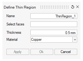
- the Name: by default, a name is suggested with an automated numbered index. Renaming is allowed, even after its creation.
- the Select faces: allows to define the thin regions.
The selection can be made on:
- Meshed faces of a solid body directly in the interface.
- Shell bodies with a surface mesh from the Assembly tree.Note: If a shell body contains multiple faces, it will select all of them.
- The Thickness: parameter defining the thickness value
of the thin region. In this context, the thin region is treated as a
mid-surface, meaning that the solver will consider half of the thickness
above the thin region and the other half below it.Important: To obtain accurate results, it is crucial for the thickness to be significantly smaller than the length and the width of the thin region.
- The Material: allows to select a material from the list of all materials defined in the solution. Thin region load works only with conductive material.