Check a component pin clearance with various objects on design.
Test Component Definition: Select checking target components.
All: Target component will all on design.
Excluding Component: If you do not want to check for certain
components from all components, define them by selecting from the
component group list.
Component Group: If you want to select target components from the
list, use this menu.
Checking
Target Layer Selection: Depending on layer selection, tables setting
will be different. Table setting will affect Routing Pattern
Clearance and Copper-Pour Clearance. For All Layers will be
applicable to all layers. And using selection, For Individual Layer,
you can individually set different clearance rules for top, bottom,
or inner layer.
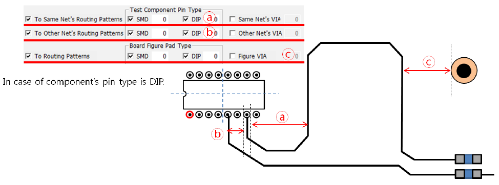
Routing Pattern Clearance
Set All Clearance: Assign all clearance values with given
values.
To Same Net’s Routing Patterns: Set the clearance value
between specifying type of the component pin pad and same
net routing patterns.
To Other Net’s Routing Patterns: Set the clearance value
between specifying type of the component pin pad and other
net routing patterns.
To Routing Patterns: Set the clearance value between board
figure via and routing pattern. Figure 1.
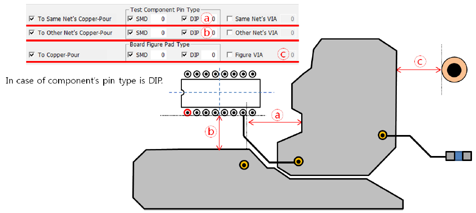
Copper-Pour Clearance
Target Net Name: Assign net name. PollEx DFM checks only copper-pours with
specified net names. Multiple net names will be divided with
a comma (,).
To Same Net’s Copper-Pour: Set the clearance value between
specifying type of the component pin pad and same net
copper-pour.
To Other Net’s Copper-Pour: Set the clearance value between
specifying type of the component pin pad and other net
copper-pour.
To Copper-Pour: Set the clearance value between board figure
via and copper-pour. Figure 2.
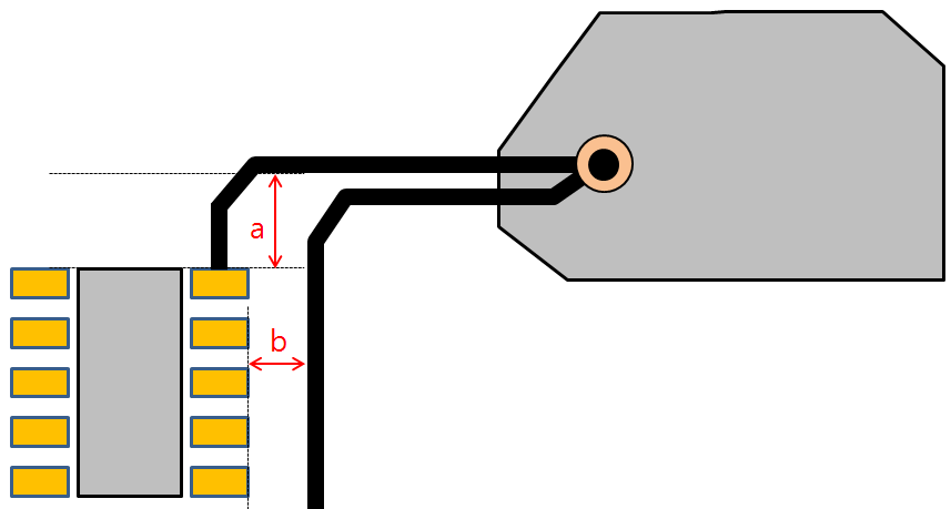
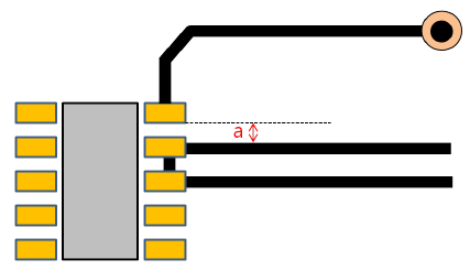
In Same Net Checking, do not check for Pad Connected Net’s Segment:
This option is a void-checking option. If you run this option,
PollEx DFM does not check the same net
pad connected net segment. Figure 3.
In Figure 3, even though the result of measuring a and b
violate the input condition, in a case, the net segment is directly
connected to pad. So, only the b case will be fail. Checking target
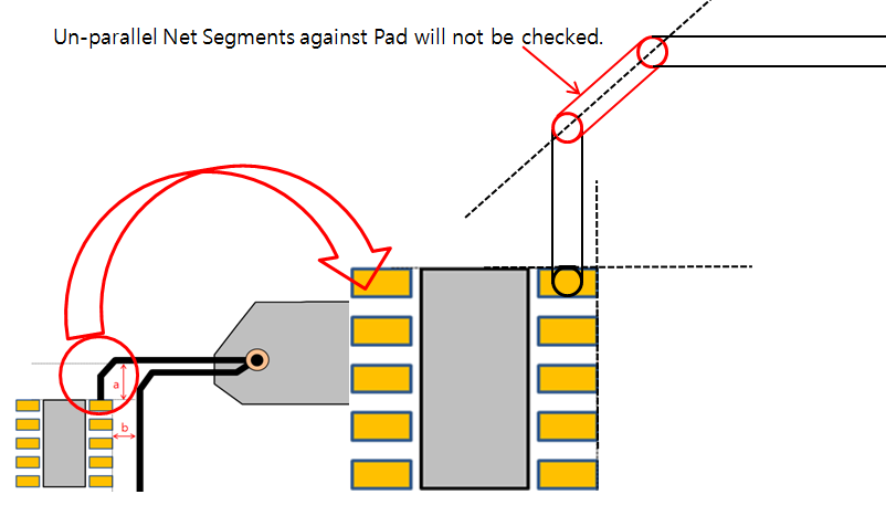
net segments will be parallel along pads side directions. Figure 4.
Do not check Net Segments under Pad Area: This is also a
void-checking option for net segments passing through under pad
area. Figure 5.
In Figure 5, checking a violates input condition. However,
because the violating net segment is lying under the pad area, this
will be passed in checking.
Exclude checking for NC pins connected to specific nets.
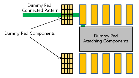
Exclude Checking for Dummy Pad Connected Net: This is another
void-checking option for routing pattern, connected to dummy
pad. Figure 6.
Dummy Pad Component: Set dummy pad component group.
Dummy Pad Attaching Component: Set dummy pad and connected
component group.