Keep Out Pattern
Check routing status from certain components.
If signal pattern under certain components can make electrical or mechanical problem,
you can define keep-out area from components.
- Checking for pattern existence in component area:
- Item: Specify the item name.
- Component Group: Select target components from the component group list.
- Component Boundary: Select component boundary criteria among pad, Component Overlap Checking Area (COC), silkscreen, silkscreen + pad, Measure (definition in component classification dialog), and PAD Inside (Pads’ inside area).
- Expand Component Boundary: Component boundary expanding area. To define expanding distance, set the expanding distance value.
- Contitional Layer: Option to define a area which will be recognized as a keepout area that overlapped with the keepout components.
- Target Layer: Define target layers.
- Component Placed Layer: Same with component placed layer will be target layer. Meaning, if component placed on top layer, patterns on top layer will be checked.
- Opposite Layer: Layer which is opposite the component placed layer will be target layer.
- Inner Layer: Inner layer pattern will be checked.
- All: Check all inner layers.
- From Component Placed Layer: Check the specified number of inner layers from the component placed layer.
- From Opposite Layer: Check the specified number of inner layers from the opposite side of the component placed layer.
- Target Object Definition: Define target objects for checking.
- Copper: If copper-pour exists in checking area, it will be detected.
- Trace: If routing patterns exist in checking area, it will
be detected.
- Minimum Trace Width: Define minimum trace width for checking.
- Maximum Trace Width: Define maximum trace width for checking.
- Through Via: If Through Via exists in checking area, it will be detected.
- Blind Via: If Blind Via exists in checking area, it will be detected.
- Buried Via: If Buried Via exists in checking area, it will be detected.
- Target Net
- Same Net: Patterns with the same net name with pins will be target routing patterns. In this option, different net name pattern will not be checked.
- Other Net: Patterns with different net name with pins will be target routing patterns. In this option, same net name pattern will not be checked.
- Specific Net: Option to check specific nets by using string filter.
- Except Net Name Filter: Option to exclude certain Net from checking by using string filter.
- Void-Checking Component Group: Select void-checking components with
selecting components group list. Void-Checking components would be
eyelet components or heatsink.
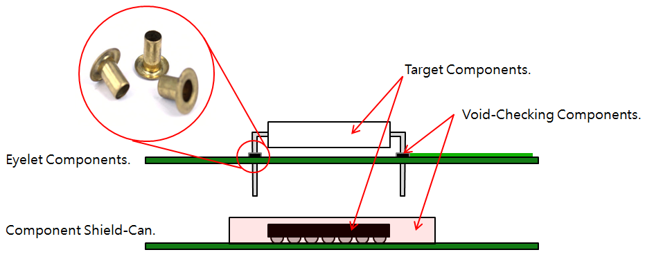
Figure 1. - Distance from void-checking Comp: For patterns connected to void-checking components within given distance from void-checking components, PollEx DFM skips to check them.
- Checking for pattern existence between adjacent pins: Check patterns between
two adjacent pins.
- Item: Specify the item name.
- Comp Group: Select target components from component group list.
- Target Layer: Define target layers.
- Component Placed Layer: Same with component placed layer will be target layer. Meaning, if component placed on top layer, patterns on top layer will be checked.
- Opposite Layer: Layer which is opposite with the component placed layer will be target layer.
- Inner Layer: Inner layer pattern will be checked. Select the inner layer physical layer number.
- Same Net: Check patterns with the same net name with connected pins.
- Other Net: Check patterns with the same net name with connected pins.
- Copper: If copper-pour exists between two adjacent pins, it will be detected.
- Trace: If routing patterns exist between two adjacent pins, they will be detected.
- Via: If via exists between two adjacent pins, it will be detected.
- Checking Area reduction Ratio(%): Option to reduce the target pin and pin area by the entered ratio from checking.
- Except Net Name Filter: For void-checking routing net selection, use net name filter. Use net name filtering tool.
- Clearance between target component nets.
- Item: Specify the item name.
- Comp Group: Select target components from component group list.
- Component Boundary: Select component boundary criteria among pad,Measure (definition in component classification dialog) Component Overlap Checking Area (COC), silkscreen, silkscreen + pad, and COC+Pad.
- Target Layer: Define target layers.
- Component Placed Layer: Same with component placed layer will be target layer. Meaning, if component placed on top layer, patterns on top layer will be checked.
- Opposite Layer: Layer which is opposite with the component placed layer will be target layer.
- Inner Layer: Inner layer pattern will be checked. Select the inner layer physical layer number.
- Check Option: Specify the check option.
- Clearance: The value inputted by the user is recognized as Net Clearance and expressed in the form of "Clearance:Value" in the Check Option column.
- Set clearance value with the shortest distance between pads: Recognizes the shortest pad distance of the part to be checked as Net Clearance, expressed in the form of "Shortest distance between Pads" in the Check Option column.