Crack Pattern
In almost cases, pattern connected to pin should be thicker than a certain width and should keep its thickness within a certain distance.
Because PSR is opened at solder-mask area, the thin thickness of pattern is weak from
external impact.
- Checking
- Item: Specify the item name.
- Component Group: Select target components from the component group list.
- Exclude Component Group: Select void-checking components from target components by selecting component group from the list.
- Max Pad Size: Set the pad size to be designated as the inspection target in the set part. Inspect if the pad is smaller than or equal to the set value. (The pad size is based on the long axis).
- Criteria: Select criteria to define pass or fail.
- Minimum: If a target component pattern is thinner than the given width, it is fail.
- Maximum: If a target component pattern is thicker than the given width, it is fail.
- Same: If a target component pattern has the same width as the given width, it is fail.
- Pattern Width: Specify the target pattern width for checking.
- Distance: Define the pattern width keeping distance from the pad
edge. If the pattern doesn’t keep certain width within the given
distance, it is fail.
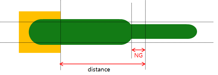
Figure 1. - Pass/Fail Option: If multiple patterns are connected to one pin and
even if a pattern satisfies the given condition, all connected
patterns are passed.
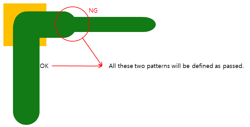
Figure 2.