SL Card
This card defines, for the combined MoM/MTL, the transitioning point from circuit elements (defined in a cable schematic) to the full wave model (defined using DP cards).
In the Solve/Run tab, in the Cables group,
click the ![]() Schematic link
(SL) icon.
Schematic link
(SL) icon.
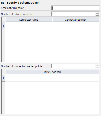
Parameters:
- Schematic link name
- The name of the interface definition between the schematic and the 3D full wave model.
- Number of cable connectors
- The number of cable paths terminating in the schematic link.
- Connector name
- The path start/end connector name. Start and end points of a cable path section are uniquely identified using the Connector at start and Connector at end labels at the CS card.
- Connector position
- The name of the data point coinciding with the path start/end connector name (defined at the CS card).
- Number of connections
- The combined number of geometric connections between the circuit elements and the full wave model. A connection can be either to a mesh vertex or a port.
- Point
- The name of the point connected to the full wave model (mesh vertex defined using the DP card). The mesh vertex point can be either a metallic triangle vertex, segment vertex or PEC infinite ground plane (defined using the BO card).
- Port
- The name of the port connected to the full wave model (defined using the PT card). The port negative terminal should coincide with the reference surface.
- Number of reference labels
- The number of labels defining the common reference surface, translating to a single node of reference on the cable schematic.
- Reference label
- The name of the label(s) defining the common reference.Note:
- If one of the connections references a port, a reference label is required.
- If none of the connections references a port, a reference label is optional.
- Include ground plane as reference
- Select this check box to include the ground plane as part of the common reference
surface, translating to a single node of reference on the schematic.Note: The triangles (labels) and PEC ground plane that define the cable schematic link common reference surface should not be disjoint.