Width
This rule checks routed trace widths against the specified minimum or maximum allowable widths.
Ideally, a transmission line has no resistance. However, when calculating the electrical performance of a printed circuit board, one must consider the attenuation losses and signal distortion from transmission lines caused by the resistance of the conductor. In addition, with the operating voltage levels getting lower, the resistance of the conductor is becoming more important to system performance.
When analyzing resistance for the purpose of PCB performance it is common to calculate the maximum DC resistance of a conductor. The minimum conductor width and minimum copper thickness should be used when calculating maximum resistance.
- Item: Input item name.
- Net: Select a target net group.
- Start Component/End Component: A test will be performed between the start component and end component.
- Net2: Check the total path including middle component.
- Middle Comp: Upon selecting this component, if the middle component exists between the start component and the end component, you can check the total path including the middle component. The middle component can be an active component.
- Component Keep IN/OUT: Define the test region. For example, you can test
inside or outside the breakout region of CPU with different test values.
Double-click the blank field. The Component Keep in/out Setup dialog
displays.
- Component Keep in/out:
- Component Group: Select the required component group which is used for defining the test region.
- Region: Define the required test region.
- IN: DFE tests the inside of the breakout region of the target component.
- OUT: DFE tests the outside of the breakout region of the target component.
- Range (COC+distance): Enter the distance value to define the breakout range. The COC (Component Overlap Check) plus this distance value is considered the test range.
- Different Rule Setup in Special Region: Assign an additional test region for breakout region testing.
- Extended Region from COC: Enter the distance value to define additional range. The COC (Component Overlap Check) plus this distance value is considered the additional test range.
- Allowable Values: Assign an additional allowable test value for this
additional region. Upon clicking
 , the DFE Input
Floating Point Value Setting dialog displays. You
can assign multiple additional allowable values in the
dialog.
, the DFE Input
Floating Point Value Setting dialog displays. You
can assign multiple additional allowable values in the
dialog.- Value: Add additional allowable values.
- Range: Add additional allowable ranges.
- Deviation: Add additional allowable values with deviation.
- Deviation (%) Add additional allowable values with deviation (%).
Test Range and Values
- Case 1: Component Keep In Region Test
-
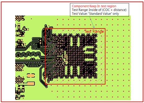
Figure 1. - Case 2: Component Keep Out Region Test
-
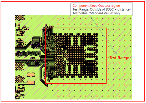
Figure 2. - Case 3: Component Keep Out with Extended Region Test
-
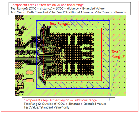
Figure 3.
- Limit: Select a rule type.
- Segment Width: Assign reference trace width.
- Each Layer: Define different width values for different layers.
- Layer No.: Define layer number. If you do not enter any specific value, the
DFE gets the layer number from PCB property by default.
- Width (Each Layer): Define different width values for different layers.
- Width: Required width for each layer.
- Use Default Value: The DFE uses the longest net’s width by default. (per layer)
- Pin Escape: Enter a radius of circular region around pins to be excluded for the rule check.
- In some cases, trace width and clearance rules are contradicting between manufacturing concern and electrical performance concern. Therefore, DFM and DFE rules must be considered at the same time.
Determine Minimum Trace Width Requirement

Figure 4.
Since the maximum allowable current for a PCB pattern is 1,000 mA/mm, power pattern should be bigger than 0.5 mm to flow 500 mA and it can be calculated as:
1,000 mA: 1 mm = 500 mA: X
X = 1mm * 500 mA / 1,000 mA = 0.5 mm