Lately, the use of inner via becomes more common. Many high-speed signals are routed
in inner layers and connected to through-hole vias and leaving top and/or bottom via
pads unconnected. This makes a so-called via stub and it will also be a good
antenna. In high-speed design, via stub can create or receive noise from other
routing structures because it acts as an antenna. The stubs can be avoided by
routing only Microstrip traces on the top and bottom layers of the board. However,
this might not be possible because of layout constraints, EMI related concerns, or
other board design considerations with Microstrip traces. This rule checks whether
there is such via stub that causes an EMI concern.
Except Net for Check: PollEx DFE does not check for
vias connected to these net groups.
Number of Remained Layer: Define via stub layer count to be treated as an
antenna.
Check Dangling VIA: Check that if there exist via that has no net
connection.
Except Via: Select vias to be excluded for this rule checking.
Padstack Name: Select via using Padstack Name.
Padstack Size: Select via using Padstack Size.
The report of this rule check includes antenna structure vias and their
locations.
For those reported vias, you can view their structures with PollEx Net 2D/3D viewer to investigate more details.
In low frequency, via stubs do not cause many problems. But in high frequency, they
can create or receive noise from other routing structures because they act as
antenna.
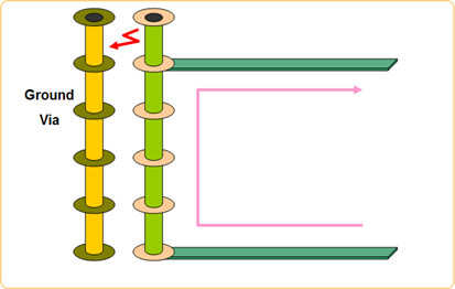
By placing a ground or ground via beside antenna via, you can reduce unwanted effect
of via stub. Figure 1.
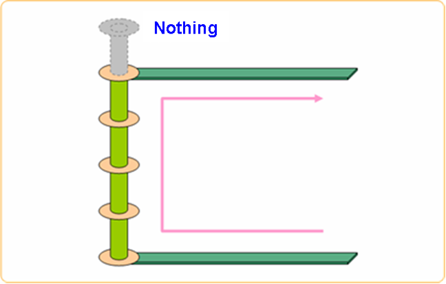
Another method is to remove via stub by using BB-via (blind via or buried via) that
is more expensive to manufacture than through-hole via. Figure 2.
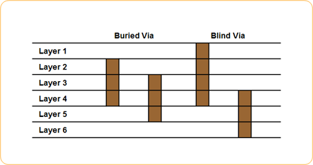
Via Types
There are types of via that help reduce EMC concerns caused by via stubs.
Micro via
Hole diameter is usually under 100μm and it is used as a pad for
discrete components. It occupies small space on board and reduces
power/ground cutting effect which is caused by large via. Instead of
using large vias, you can replace them with micro via to reduce
inductance at connecting positions.
Buried via
This via exists only in inner layers. It cannot be visually observed
from top or bottom. It is usually used in high speed signal board to
prevent Power/Ground Cutting Effect and also give PCB designer
additional spaces for routing.
Blind via
This via connect from top or bottom to inner layer only. So, this via
could be seen only from top or bottom. When it is used with blind via,
it is very effective in cost and routing space control.