Net to Net
This item checks whether a specified clearance requirement for the net is satisfied.
- Auto Net to Net Combination: Generate combination pair of selected net group.
- Item: Input item name.
- 1st Net: specify 1st net (reference).
- 2nd Net: specify 2nd net (target net).
- Type: Define separation measure base.
- Value: The clearance value in Strip Clearance, Microstrip Clearance, Strip Clearance with Pad/Via and Microstrip Clearance with Pad/Via are considered as Separation Value.
- Width: The value in Strip Clearance, Microstrip Clearance, Strip Clearance with Pad/Via and Microstrip Clearance with Pad/Via are considered as multiple of Pattern Width.
- Strip Clearance: Enter trace-to-trace clearance for stripline (traces on inner signal layers).
- Microstrip Clearance: Enter trace-to-trace clearance for microstrips (traces on top and bottom layers).
- Stripline Clearance with Pad/Via: Enter trace-to-pad or trace-to-via clearance for stripline.
- Microstrip Clearance with Pad/Via: Enter trace-to-pad or trace-to-via clearance for microstrips.
- Net Exception: Check clearance between 1st Net group and all other signals exclude 2nd Net group.
- L1 Clearance: Enter clearances from the reference layer to the one layer above and below.
- L2 Clearance: Enter clearances from the reference layer to the two layers above and below.
- Pin Escape: Enter a radius of circular region around pins to be excluded for the rule check.
- Area Layer: Select the artwork layer to be checked. PollEx DFE recognizes check areas defined by polygon or polyline.
- Area Clearance: Enter a clearance to the region that is defined in Area Layer.
- Component Keep IN/OUT: Define the test region. For example, you can test inside or outside the breakout region of CPU with different test values.
- Component Keep in/out:
- Component Group: Select the required component group which is used for defining the test region.
- Region: Define the required test region.
- IN: Test inside of the breakout region of target component.
- OUT: Test outside of the breakout region of target component.
- Range (COC+distance): Enter the distance value to define breakout range. The COC (Component Overlap Check) plus this distance value is considered the test range.
- Target Layer: Select the required test layer.
- All Layer: Test all layers.
- Component Place Layer: Test only the component placement layer.
- GND Net: DFE skip to check if ground net is existing between two target nets.
- Width base item: Only the item listed here will be affected by
option ⑤.
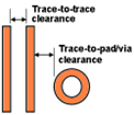
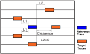 Figure 1.
In order to reduce coupling, it is best to make wider clearances for signal. However, clearances are restricted by board size and pin pitch as well as signal characteristics such as voltage or frequency. For example, a clearance among clocks is usually wider than that among normal signal nets. A clearance between clock and normal signal net is also wider than that among normal signal nets.
Clearances among signal nets must be carefully considered on the same layer as well as on adjacent layers.
| Voltage (DC or AC Peak) | Minimum distance (uncoated) | Minimum distance (uncoated) | ||
|---|---|---|---|---|
| ~ 15V | 15 mil | 0.4 mil | 5 mil | 0.13 mil |
| 15V ~ 30V | 15 mil | 0.4 mil | 10 mil | 0.25 mil |
| 30V ~ 50V | 15 mil | 0.4 mil | 15 mil | 0.4 mil |
| 50V ~ 100V | 25 mil | 0.6 mil | 20 mil | 0.5 mil |
| 100V ~ 150V | 25 mil | 0.6 mil | 30 mil | 0.8 mil |
| 150V ~ 300V | 50 mil | 1.5 mil | 30 mil | 0.8 mil |
| 300V ~ 500V | 100 mil | 1.5 mil | 60 mil | 1.5 mil |
| 500V ~ | 0.2 mil/volt | 0.005 mil/volt | 0.12 mil/volt | 0.003 mil |
A partial copy of IPC-2221 standard is shown in IPC Material for an additional example.