Net Group Shield
This item checks for a shielding ratio of bus group.
High speed design utilizes ground planes to stabilize signal transmission. However,
use of solid ground planes is restricted in miniaturized and high-density designs,
so use of partial ground plane and ground traces becomes common. Since a perfect
shielding is impossible, designers should carefully consider these in their designs.
In general, with considering pin and via usages, a minimum of 80 percent shielding
is recommended. Ground shielding should consider the effect on impedance change of
outer signals.
- Component Except Area: Define component except area.
- Component Group: Target Component Group. The DFE will exclude this area during testing.
- Except Area Type: The measure base of component group. (PAD/COC/SILK+PAD)
- Layer: The target layer in which except area should be adopted. (Component Layer/Up to Main Ground/All)
- Main Ground Count: Enter allowable M-GND count.
- Item Name: Input item name.
- Net: Define net group for shielding check.
- Shield Net: Define net group which can be a shield net. High speed signal will be shielded with nets in this Shield net group.
- Max Net Count: Signal group maximum net count limit. If the net count is greater than this value, it will not check shield ratio. (Reports the net count error messages)
- Min Group Distance: Group signal maximum separation limit. The tool groups signal lines with this separation. It means that if two signals separation is greater than this value, the tool considers two signals as two separation groups.
- Component Keep IN/OUT: Define test region. For example, you can test inside
or outside the breakout region of CPU with different test.
- Component Group: Select required component group which is used for defining the test region.
- Region: Define the required test region.
- IN: DFE tests the inside of the breakout region of target component.
- OUT: DFE tests the outside of the breakout region of target component.
- Range (COC+distance): Enter the distance value to define breakout range. The COC (Component Overlap Check) plus this distance value is considered the test range.
- Target Layer: Select the required test layer.
- All Layer: Test all layers.
- Component Place Layer: Test only component placement layer.
- Include Pin/Via: DFE checks the net separation including Pin/VIA.
- H-Exclude Component: DFE excludes the specific area which is defined at ① during horizontal shield checking.
H-Shield Check
Option for horizontal shield check.
- Horizontal Shield Ratio Check:
- Shield Distance: Distances from most nets in net group between
ground nets in GND net group.
- Use Width Value(W): The value in Shield Distance is considered as multiple of Pattern Width.
- Max: Specify maximum distance from differential pair net to ground. The DFE searches shielding net within this range.
- Min: Specify minimum clearance from net to ground. If shield net exists closer than this clearance, it reports as failed.
- Min Horizontal Shield Ratio(%): Minimum shielding net length ratio against total net. If the shielding ratio is smaller than given value, it is reports as failed. (Ratio = The total length of shielded portion of net/Total length of net)
- Shield Ratio Calculation Type: Determine shield ratio calculation method.
- All Layer: Calculate shield ratio for total net.
- Per Layer: Calculate shield ratio per each layer.
- Exclude/Include Option:
- Exclude Layer: The target layer excluded during testing. . The DFE uses relative layer number. For example, in case of 8-layer PCB, Top-1 layer means L2, Bot+1 layer means L7.
- Exclude Short Pattern: Exclude the short length trace shorter than this value.
- Exclude Pin Area (Pin Pad + Shield Distance): Define excluded area around PIN area. The DFE extends the excluded area with the same amount of specific distance from pin pad.
- Guard Via Distance Check: The DFE check maximum via distance of shielding net.
-
- Guard Via Range: Define the maximum distance from trace edge within which guard via should be exist. The DFE considers only the vias within this range as a guard via.
- Max Via Distance: If the via distance is greater than this value, it is reported as failed.
- Except PAD: Exclude pin pad for testing.
- Merge Result Via Count: PollEx DFE shows the merged result of all errors on the same display.
- V-Exclude Component: DFE excludes the specific area which is defined at ① during vertical shield checking.
- Shield Distance: Distances from most nets in net group between
ground nets in GND net group.
V-Shield Check
Option for vertical shield check.
- Vertical Shield Ratio Check:Shield Distance (Extended V-Shield Width): Specify minimum required GND width of upper/below layer.
- Min Vertical Shield Ratio(%): Minimum ground shielding ratio. If the shielding ratio is smaller than given value, it is reported as failed. (Ratio = Shield Area/Net Area)
- Exclude/Include Option:
- Exclude Layer: The target layer excluded during testing. The DFE uses relative layer number. For example, in case of 8-layer PCB, Top-1 layer means L2, Bot+1 layer means L7.
- Check Layer:
- L1 Layer: check one layer above and below.
- L2 Layer: check two layers,one layer apart above and
below.
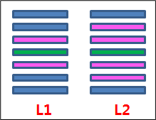
Figure 1.
- Pin Escape: Enter a radius of circular region around pins to be excluded for the rule check.
- Via Escape: Enter a radius of circular region around vias to be excluded for the rule check.
- Exclude Short Pattern: Exclude the short length trace shorter than this value.
- Exclude Short Un-Shielded Length: Exclude the short length un-shielded trace shorter than this value.
- Consider the same net as a shield-net.
- Exact net shape: DFE considers the same net as a shield net.
- MinMax of net Group shape: Extend Range: Extend the check range by the Extend Range from the outermost of the Net Group to be checked, and if there is the same net on the vertical layer, it is considered a Pass.