3D IC
![]()
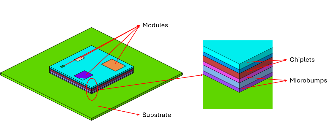
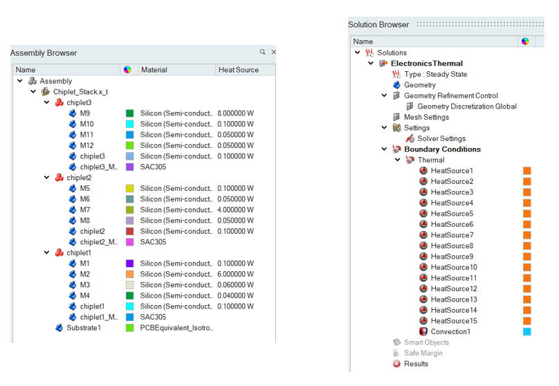
In the electronic design automation field, a floor plan of an integrated circuit refers to a tentative placement diagram of its major functional blocks. The location of these blocks is a crucial aspect of floor planning, as it will have a significant impact on the overall performance of the design. The power consumption of each block within the system differs, leading to varying temperature distributions around them. This tool is used to set up the complete floorplan solution with chiplet stack and necessary boundary conditions like heat source, convection and materials.
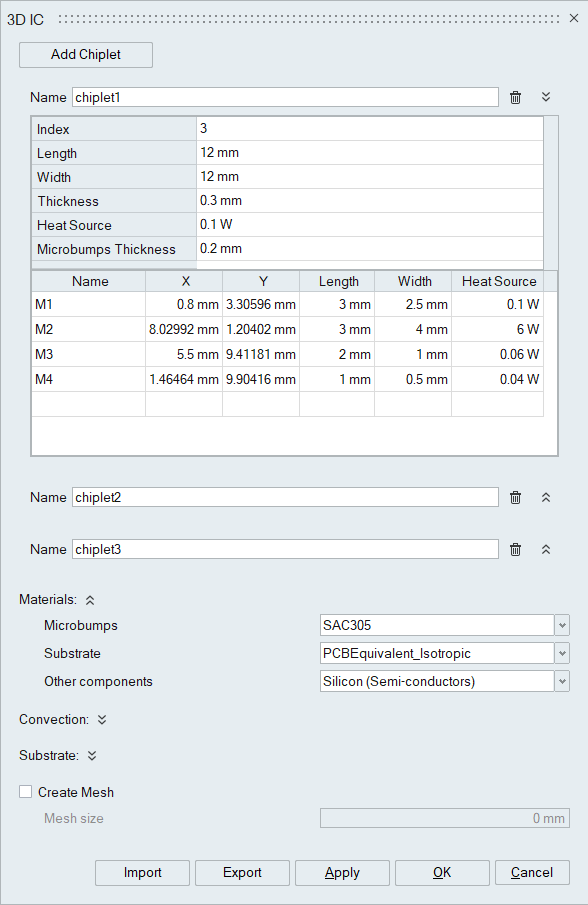
Add Chiplet
Creates a new chiplet field in the dialog box where the chiplet and module parameters can be specified.
Index
Define the stack index for the chiplet, which specifies the sequence in which the chiplets are placed vertically.
Length
Define the length (x-length) of the chiplet.
Width
Define the width (y-length) of the chiplet.
Thickness
Define the thickness (in z-direction) of the chiplet.
Heat source
Define the heat source for the chiplet.
Microbumps Thickness
Define the thickness of the microbumps.
Materials
Select the material for the microbumps, substrate, and other components from their respective drop-down menus.
Convection
Define the ambient temperature and heat transfer coefficient values.
Substrate
Define length, width and thickness for the substrate.
Create Mesh
This option helps to create the fem(meshed) model.
Mesh size
Specify the mesh size to be used.
Import
Imports the XML file containing all the chiplet information.
Export
Exports all the chiplet information to an xml file.
Create Parameters
A new option has been added in the dialog that allows you to automatically generate parameters for all fields in the dialog. This includes parameters for chiplets/modules as well as all other related inputs.
When you click Create Parameters, the software will:
- Create parameters for every editable field in the dialog
- Assign parameter names based on the corresponding field names
- Enable easier scripting and automation.
Example