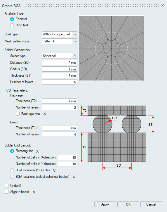
Create
![]()
Description
This tool is used to create BGA (Ball Grid Array) for both thermal and drop test analysis.
Analysis TypeThermal and Drop test are the two types of analysis.
BGA typeBelow are the different types of BGA supported.
- Without copper pad
- Solder mask defined (SMD) pad
- Non-solder mask defined (NSMD) pad (for Thermal only)
- SMD on top and NSMD on bottom (for Thermal only)
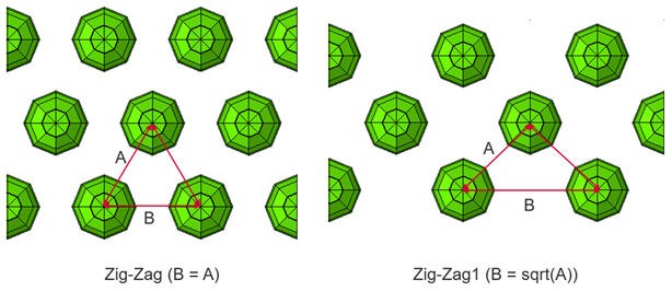
Ball pattern type
Below are the two types of patterns in which balls are placed between top and bottom plate. This is supported only for drop test analysis.
- Regular
- Zig-Zag
- Zig-Zag1
There are different types of predefined mesh pattern available.
Solder parameters- Solder type
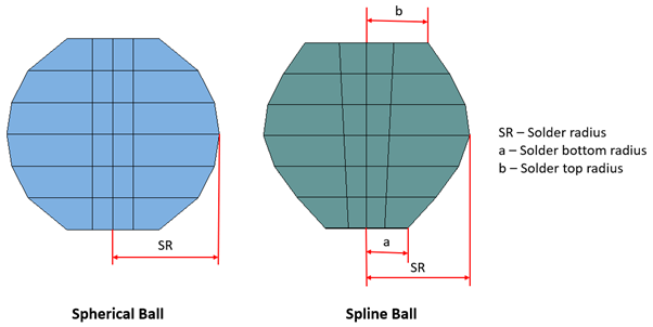
Below are the supported ball types.
- Spherical
- Spline
- Distance(SD): Distance between two adjacent balls.
- Radius(SR): Radius of the solder ball.
- Top radius: Top radius of the solder ball. (For Spline type)
- Bottom radius: Bottom radius of the solder ball. (For Spline type)
- Thickness(ST): Thickness or height of the solder ball.
- Number of layers: Number of layers of elements along axial direction of the ball.
- Solder neck thickness(NT): Thickness of solder neck. (For Copper pad embedded on the bottom side)
- Number of layers(Neck): Number of layers of elements in solder neck. (For Copper pad embedded on the bottom side)
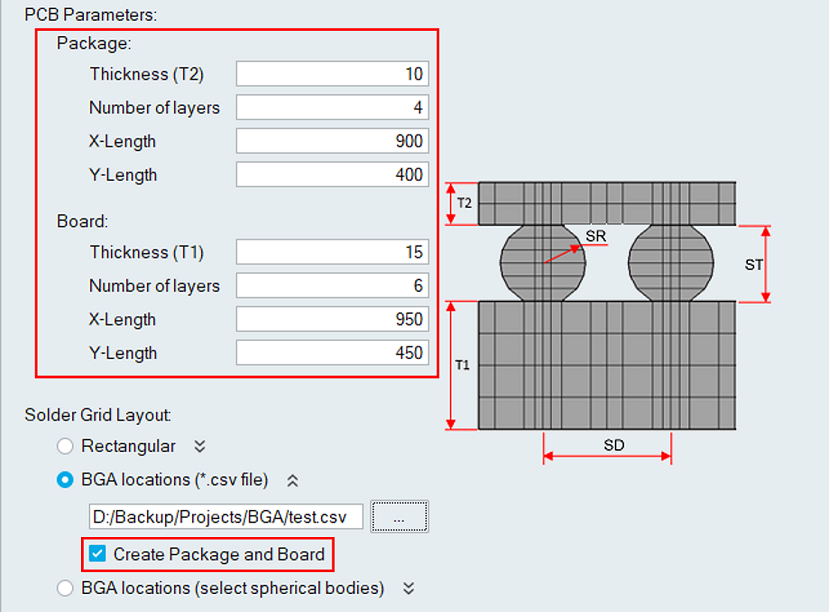
PCB Parameters
- Package
- Thickness(T2): Thickness of package.
- Number of layers: Number of layers of elements along axial direction.
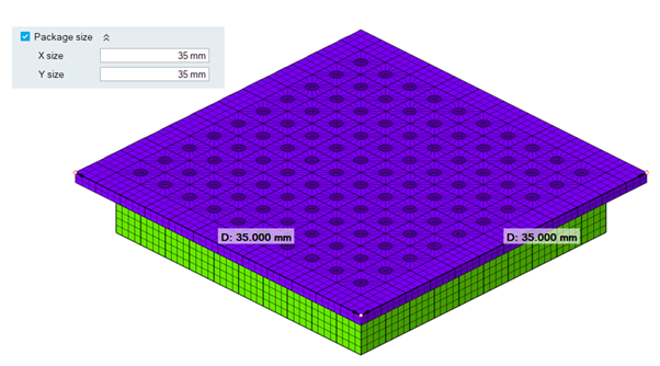
- Package size: User can specify X and Y dimensions for the package.
- X-Length: Package length in x-direction.
- Y-Length: Package length in y-direction.
- Board
- Thickness(T1): Thickness of board.
- Number of layers: Number of layers of elements along axial direction.
- X-Length: Board length in x-direction.
- Y-Length: Board length in y-direction.
- Thickness
- Top(T4): Thickness of top copper pad.
- Bottom(T3): Thickness of bottom copper pad.
- Number of layers: Number of layers of elements along axial direction.
Solder Grid Layout
- Rectangular
- Number of balls in X-direction: It specifies the number of balls in x-direction.
- Number of balls in Y-direction: It specifies the number of balls in y-direction.
- BGA locations (*.csv file)
CSV file with ball centroid data is imported to create BGA. A new toggle named ‘Create Package and Board’ is added to support creating the package and board. When the toggle is turned ON, the package and plate parameters will be enabled where the user can enter the value to each parameter.
-
BGA locations (Select spherical bodies)
This option allows you to select a set of bodies to create the BGA.
The selected bodies can be spherical or cylindrical in shape.
- If the body is spherical, a spherical BGA will be created.
- If the body is cylindrical, a cylindrical BGA (copper pillar) will be created.
Note:Materials from the input bodies are automatically transferred to the output bodies during BGA creation. By default, Copper_Pure material is assigned to the top and bottom copper pads.
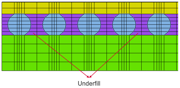
Underfill
An extra body which surrounds the solder balls between top and bottom plate will be created.
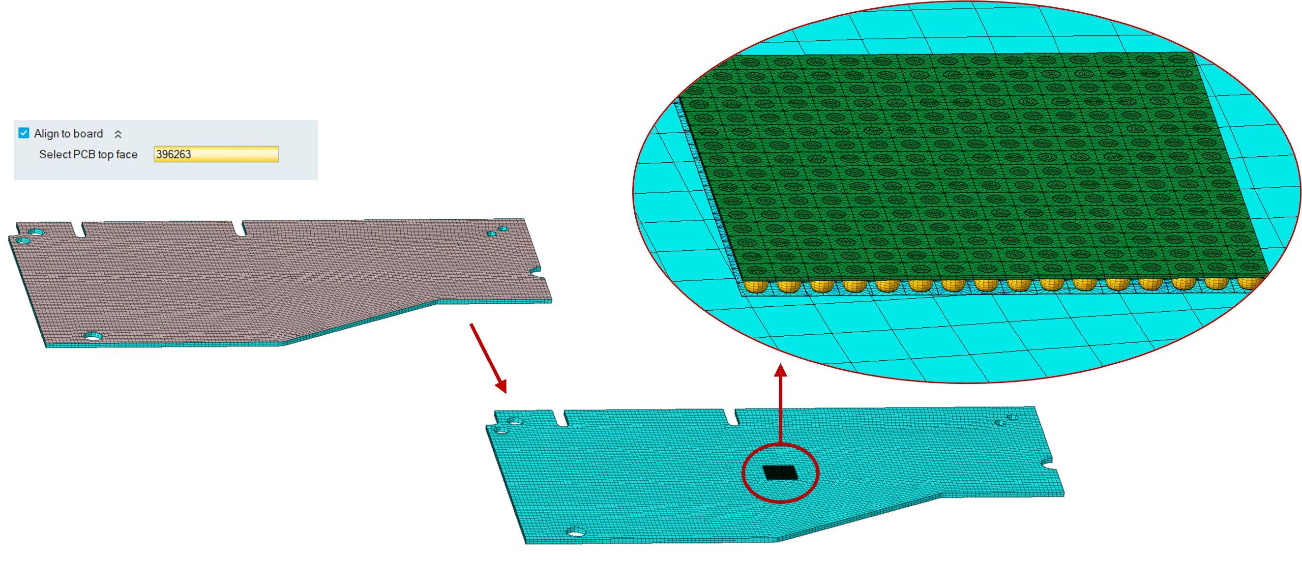
Align to board
This option is used to align the BGA on top of the PCB and the BGA bodies will be created in the input PCB model.
Examples:
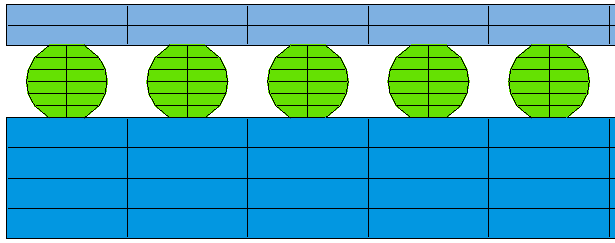
Thermal - Without copper pad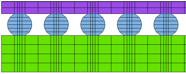
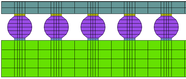
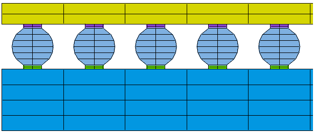
Thermal - Solder mask defined (SMD) pad
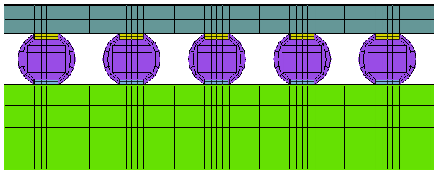
Thermal - Non-solder mask defined (NSMD) pad
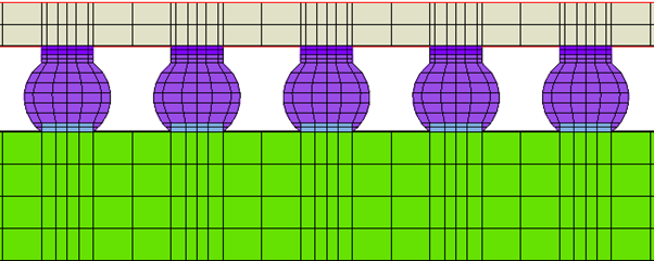
Thermal - SMD on top and NSMD on bottom
Drop Test - Without copper pad
Drop Test - Solder mask defined (SMD) pad
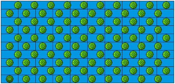
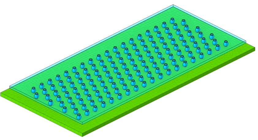
Drop Test - Regular ball pattern
Drop Test - zig-zag ball pattern
Drop Test - zig-zag1 ball pattern
Thermal - Without copper plate + Underfill
Thermal - Package size for Top plate
BGA locations (*.csv file) | Create Package and Board = ON
Align to board
Copper pillar support