Etchback
Check for the etching process that removes the wiring connected to the electroplating on the pad during the package manufacturing process.
- Etching / Plating Bar Layer Definition
- Select Etching layer for Top side: Select the etching layer drawn on the top side.
- Select Etching layer for Bottom side: Select the etching layer drawn on the bottom side.
- Select Etching layer for Inner layer: Select the etching layer drawn on the inner layer.
- Select Platting Bar layer: Select the layer where the platting bar area is drawn.
- Checking: Set the checking rules for each Top, Bottom and Inner layers.
- Minimum Etching area width: Minimum width checking of objects drawn
on the etching area.
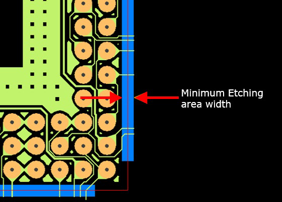
Figure 1. - Etching area Clearance to other Etching area: Minimum clearance
checking between objects drawn on the etching area.
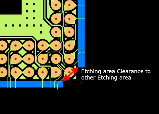
Figure 2. - Etching area Clearance to user Defined Layer Objects: Clearance checking between objects drawn in the etching area and in the user defined layer.
- Etching area Clearance to Pattern: Clearance checking between
etching area and pattern but excluding the pattern segment directly
connected to the etching area.
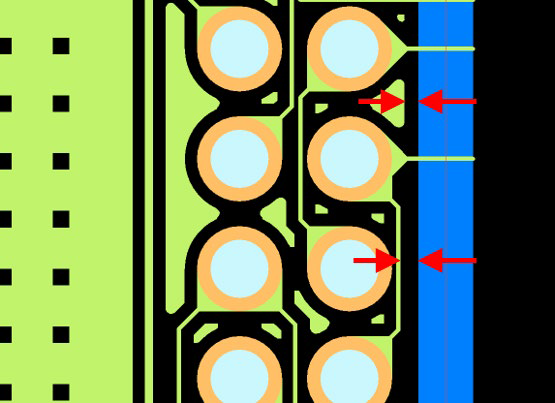
Figure 3. - Etching area Clearance to Copper: Clearance checking between etching area and copper polygon.
- Etching area Clearance to Solder Mask: Clearance checking between
etching area and solder mask.
Figure 4. - Check Pattern width in Etching area: Check whether the pattern
overlapped with the etching area is designed within the user defined
width.
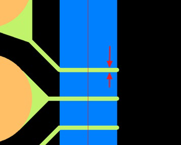
Figure 5. - Checking Plating Bar connection with Net which connected with S/R Pad: Check whether the Net connected to S/R opened pad is connected to the plating bar.
- Checking Short Nets after Etching: Check whether the shorted net exists after the etching process.
- Minimum Etching area width: Minimum width checking of objects drawn
on the etching area.