Cavity
Verify whether the Cavity area in the PCB design satisfies the design criteria.
Silicon dies might be placed on the dig out area of PCB in the package manufacturing
process.
- Cavity Definition
- Define Cavity Area from Specific Layer: Select the layer in which the Cavity area is drawn from the layer list.
- Define Cavity Layer Stack by Name Filter: Set the layer to which the Cavity is applied using the string filter.
- Die Component Definition: Select the Silicon Die component to be placed in the cavity area from the component group list.
- Checking
- Clearance to Outline: Clearance checking between Cavity area and PCB outline.
- Clearance to Other Cavity: Clearance checking between cavity areas.
- Cavity(Outer) Clearance to Pattern: Clearance checking on the outer
layers that cavity applied.
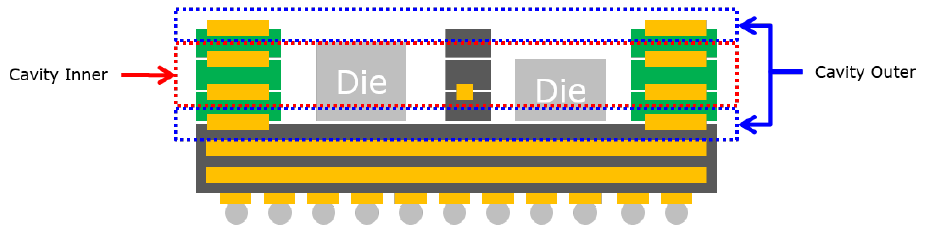
Figure 1. - Cavity(Inner) Clearance to Pattern: Clearance checking on the inner
layers that cavity applied.
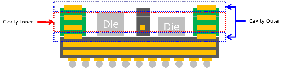
Figure 2. - Clearance to Die: Clearance checking between cavity area and COC of Die component.
- Clearance to Component
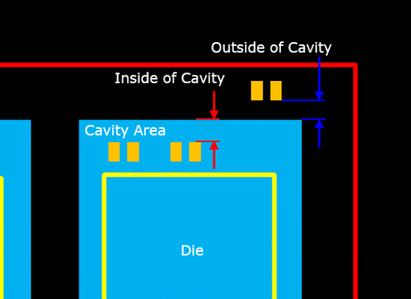
Figure 3.- Item: Specify the item name.
- Component Group: Select the target component group and cavity area.
- Measure: Select the measure base of target component.
- Inside of Cavity: Check the clearance between placed component within cavity area and cavity area (outer area).
- Outside of Cavity: Check the clearance between placed component out of cavity area and cavity area (outer area).
- Minimum Pattern Width on DIE Component placement layer within Cavity Area: Check the minimum width of the routing that passes the cavity area in the Die component placed layer.