Material Mapping
![]()
Introduction
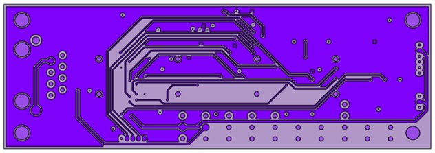
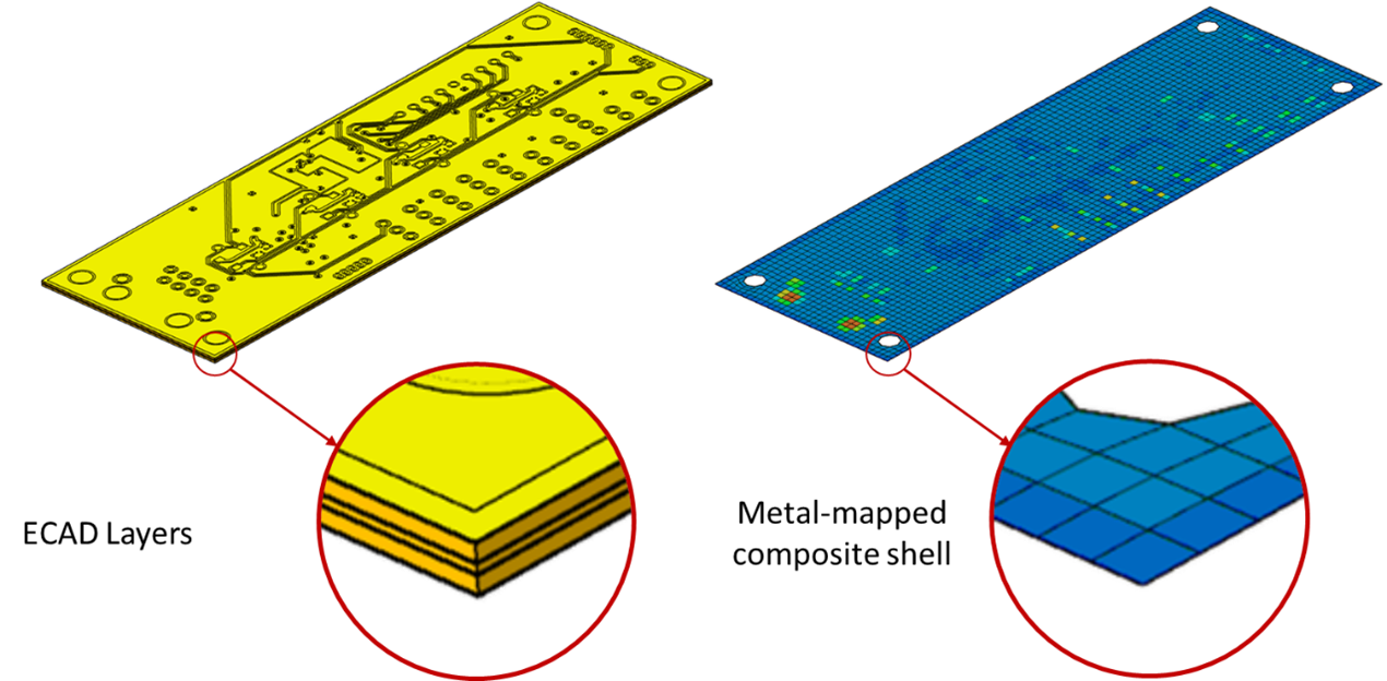
Electronic boards/substrates/dies contain thin metal traces in each layer. The meshing of the thin traces and capturing the finer feature details in the mesh will be both resource intensive and time consuming. To simplify things, we can use a course mesh by ignoring features like metal traces, vias, etc., and then account for the ignored features through proper material assignment to the elements. By this way, we could be able to save a lot of the setup and solving time without much loss in result accuracy.
This tool is used to compute equivalent material property based on the volumetric concentration of metal and dielectric in each element.
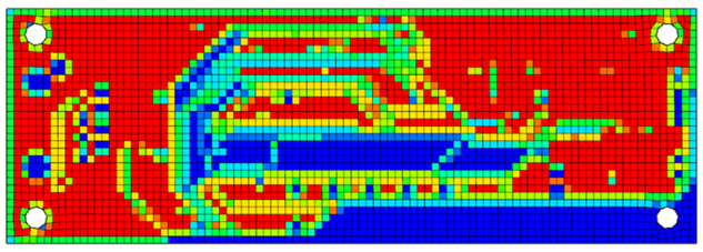
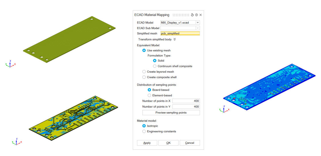
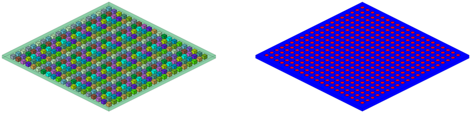
The contour below shows the concentration of the metal across a layer of a PCB model.
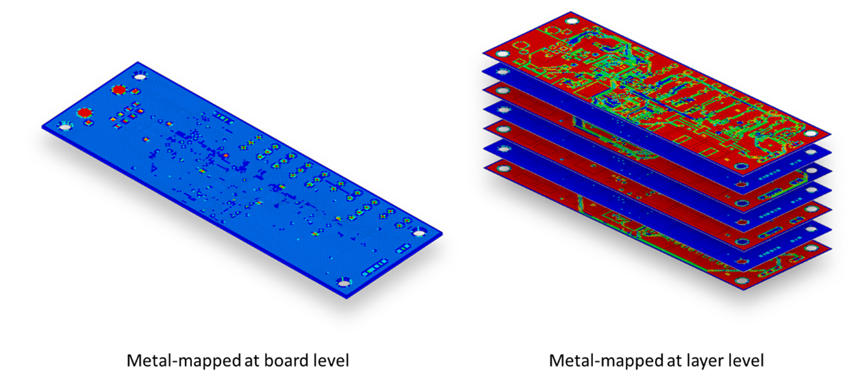
Metal-mapping can be done at both board-level and layer-level of the electronic model. It is also possible to compute and assign equivalent orthotropic properties to the shell bodies.
The same concept can be extended to interconnect structures as well. Instead of explicitly meshing individual bumps or microbumps for all simulation scenarios, their effects can be represented on a simplified reference mesh through material mapping. This approach further accelerates simulations while preserving result accuracy.
Board/Substrate/Die:
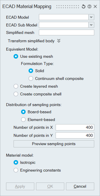
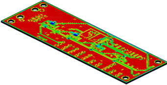
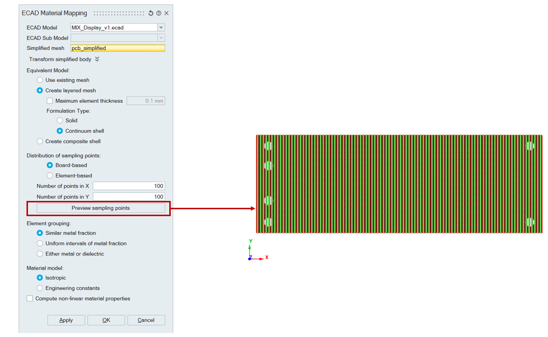
ECAD Model
Select an ECAD model to compute the equivalent material property for the given model.
ECAD Sub Model
This option allows to compute the equivalent material property of sub-models.
Equivalent Model
The equivalent material property can be computed in three ways,
- Use existing mesh
In this method, the material properties are computed at board level. Multiple reference bodies can be selected as input. There can be only one element along the thickness direction for each reference body.
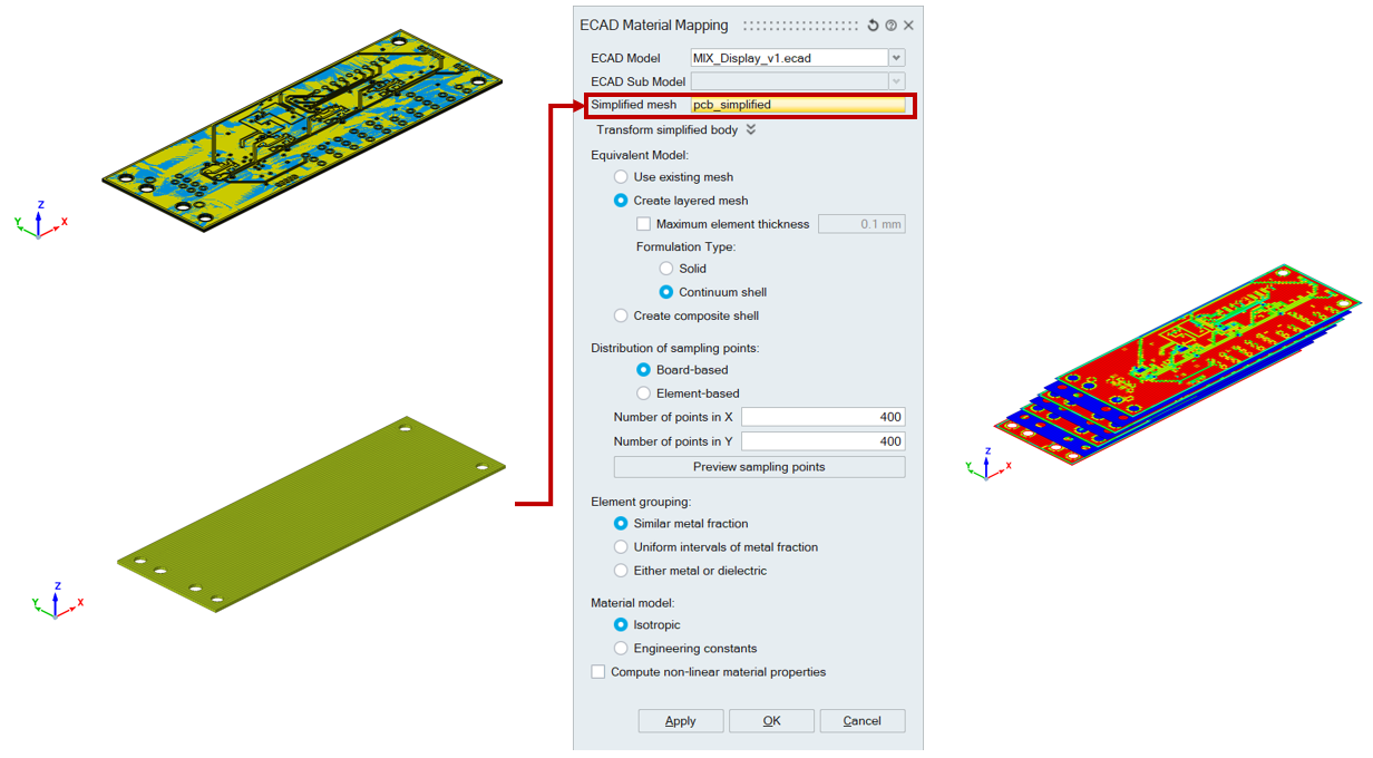
- Create Layered Mesh
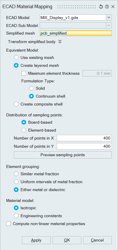
In this method, the material properties are computed at layer level. Multiple reference bodies can be selected as input. No layer approximation is considered.
Maximum element thickness:
Multiple bodies will be created with respect to the layer information present in ECAD.
If maximum element thickness is specified and if layer thickness is more than the specified value, it will create multiple hex layers.
The number of hex layers created will be equal to the ratio of layer thickness to specified maximum element thickness.
- Create Composite Shell
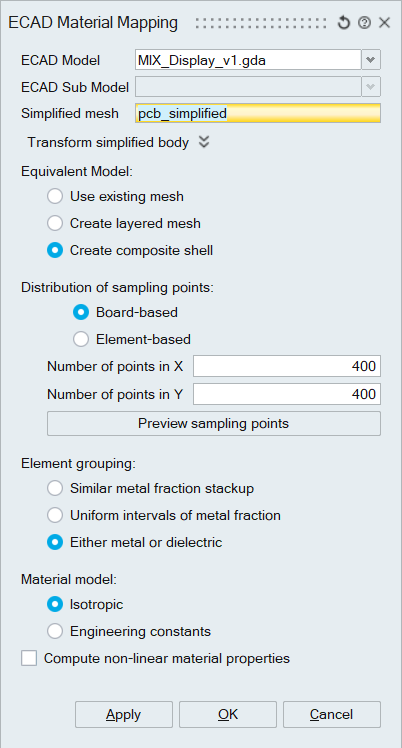
In this method, the model is approximated as a composite shell and assigned with lamina properties equivalent to the ECAD layer properties.
Element grouping
-
Similar metal fraction
Elements are grouped based on similar metal fractions and materials are assigned accordingly.
-
Uniform intervals of metal fraction
Elements are grouped into a user-defined number of metal fraction intervals.
Number of materials assigned = Number of intervals
-
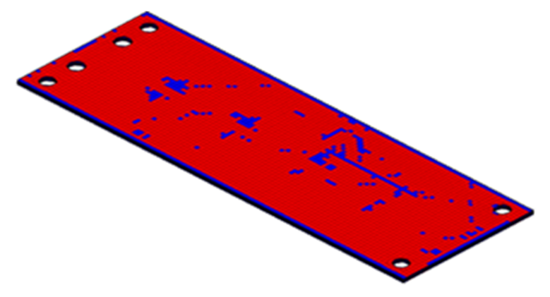
Either metal or dielectric
Elements are grouped as either pure metal or pure dielectric.
Number of materials assigned = 2
Sampling points
SimLab computes the metal fraction on the sampling points for the given ECAD model. Then the metal fraction on the sampling points is mapped to the mesh body.
It is recommended that the distance between sampling points should be smaller than the width of the trace.
Sampling points can be distributed throughout the XY plane of mesh body or on each element in the mesh body . Currently sampling points distributed throughout the XY plane of mesh body can be previewed using “Review sampling points”. Reviewing sampling points for each element is currently not supported.
Continuum Shell Approximation
By selecting this option, PCB equivalent material is computed and assigned to the body with continuum shell property instead of solid property. Continuum shells capture the bending behaviour of the PCB board a lot better. This option is available under “Combine all layers overlapping with mesh body” and “Preserve all layers” option.
Continuum Shell Composite Approximation
By selecting this option, an equivalent continuum shell composite stackup is written for each element. This option is available under “Combine all layers overlapping with mesh body”.
Transform Simplified Body
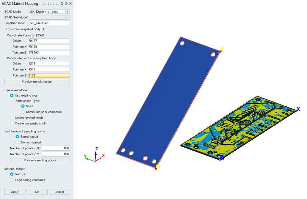
If the reference mesh body and the imported ECAD model is not overlapping, then the PCB equivalent material can be computed by selecting the reference coordinate points on the ECAD and target coordinate points on the mesh body. User can also preview the transformation before performing material mapping. If the reference mesh body and the imported ECAD model is overlapping, then this section can be left blank.
Material Models
SimLab supports isotropic and engineering constants material models for equivalent material.
- Metal fraction: Finds the metal fraction for each element and computes the material property by simple weighted average.
- Metal layout: Considers the metal fraction as well as the layout of the traces in the thickness direction and then computes the equivalent orthotropic material property for each element. This approach is used to capture the thickness direction property effectively.
If Isotropic material model is specified, metal fraction computation will be considered. For engineering constants material model metal layout computation will be considered.
Non-Linear Material Mapping
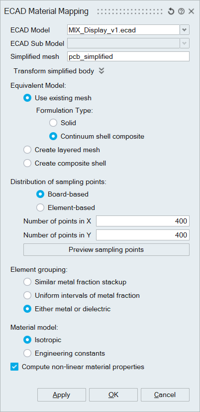
- Non-linear material mapping can be computed for the equivalent PCB.
Following material properties will be considered for material mapping.
- Density
- Youngs Modulus
- Poisson's Ratio
- Thermal Expansion
- Thermal Conductivity
- Specific heat
- Shear Modulus.
- To perform nonlinear material mapping, Materials assigned to ECAD PCB layers must be either Engineering constants or Isotropic material models.
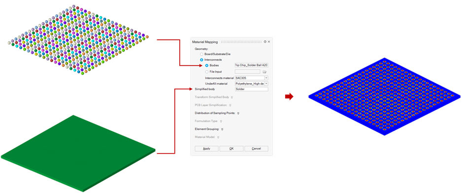
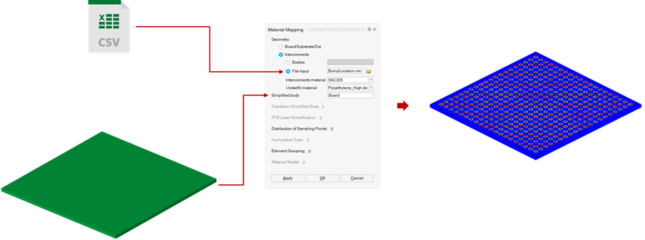
Interconnects:
Interconnect material mapping can be done based on MCAD bodies or a CSV-file.
Bodies
Select the reference MCAD bodies to compute the equivalent material property.
File Input
Select a CSV-file containing the parameters like the coordinates and radius of each bump/microbump.
- Supported for OptiStruct and Abaqus solvers only.
- Continuum shell property is applicable only for structural and coupled thermal-structural analysis.
- Continuum shell composite property is applicable only for structural analysis.
- If a body with continuum shell property is selected for thermal analysis, SimLab automatically writes out solid properties while solving.
- It is recommended to create a solution first with the reference mesh body before computing the PCB equivalent material.
- Metal mapping information will be written as separate include files for OptiStruct (SolverDeckName_MetalMappedPCB.fem) and Abaqus (SolverDeckName _MetalMappedPCB.inc)
- Nonlinear material mapping is supported only for “Create Layered mesh” technique, “Use existing mesh” technique with “Continuum shell composite” formulation type and “Create Composite shell” techniques.If “Stress – Plastic Strain” curve is specified, for copper and dielectric, plasticity data will be written for “Create Layered mesh” with “Either metal or dielectric” element grouping. If the stress-strain curve is not specified, only temperature dependent material mapping is performed.
- For interconnect material mapping, cross-section is always assumed
as a circle. If a cube body is given as reference input, circle with
equivalent cross-section area is assumed and material mapping is
performed.
- For interconnect material mapping, the reference input should always be oriented to XY-plane. If not, material mapping will not work. This is a known limitation.