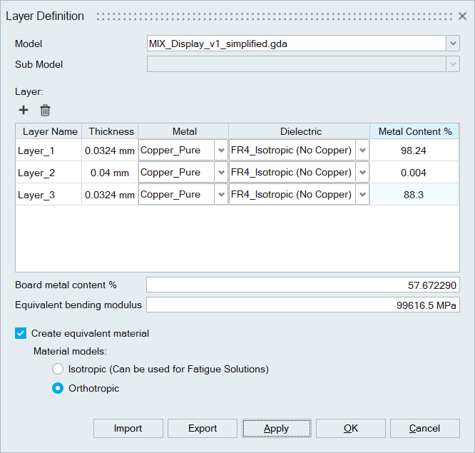
Layer Definition
![]()
Layer Definition
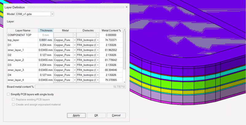
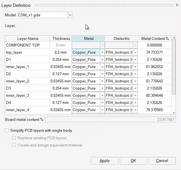
This tool is used to review and edit the layer properties of ECAD models.
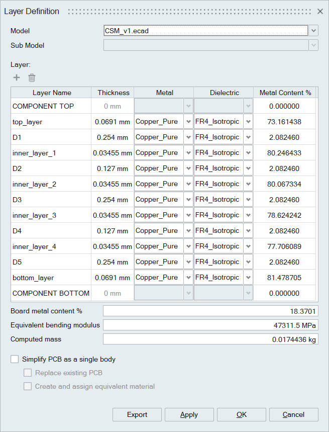
Model
Select an ECAD model to review the layer properties.
Sub Model
This option allows to review the layer information of sub-models.
Modifying the layer properties
The thickness of PCB, metal and dielectric material can be modified from the layer definition.
SimLab will classify and list the dielectric and metal materials based on the value of electrical resistivity at reference temperature under Electrical properties. If the value is less than 1e-3 Ω-m , the material is metal, else it is a dielectric material.
Simplified PCB
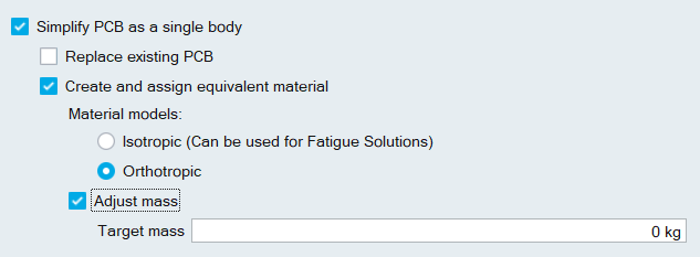
- By using "Simplify PCB layers as a single body" a single simplified PCB body can be created.
- A duplicate model with name _simplified will be created, the simplified PCB
along with the copy of the components will be available in this new model.
- In case if "Replace existing PCB" is used, the simplified PCB will be created in the same model, replacing the existing PCB layers.
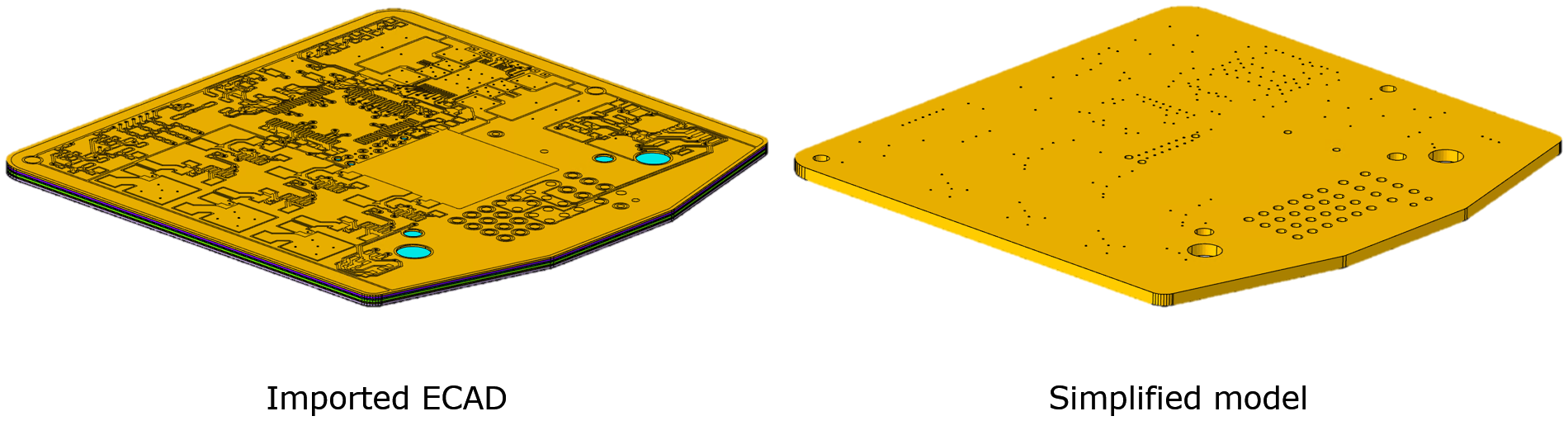
- Users can adjust the mass of the simplified PCB using adjust mass toggle and specify the target mass if the computed mass of the PCB is not satisfactory. The density of the PCB is adjusted based on the value specified in target mass. If adjust mass is not used, it will compute the density from computed mass. Adjust mass facility is not supported for manual entry of PCB data.
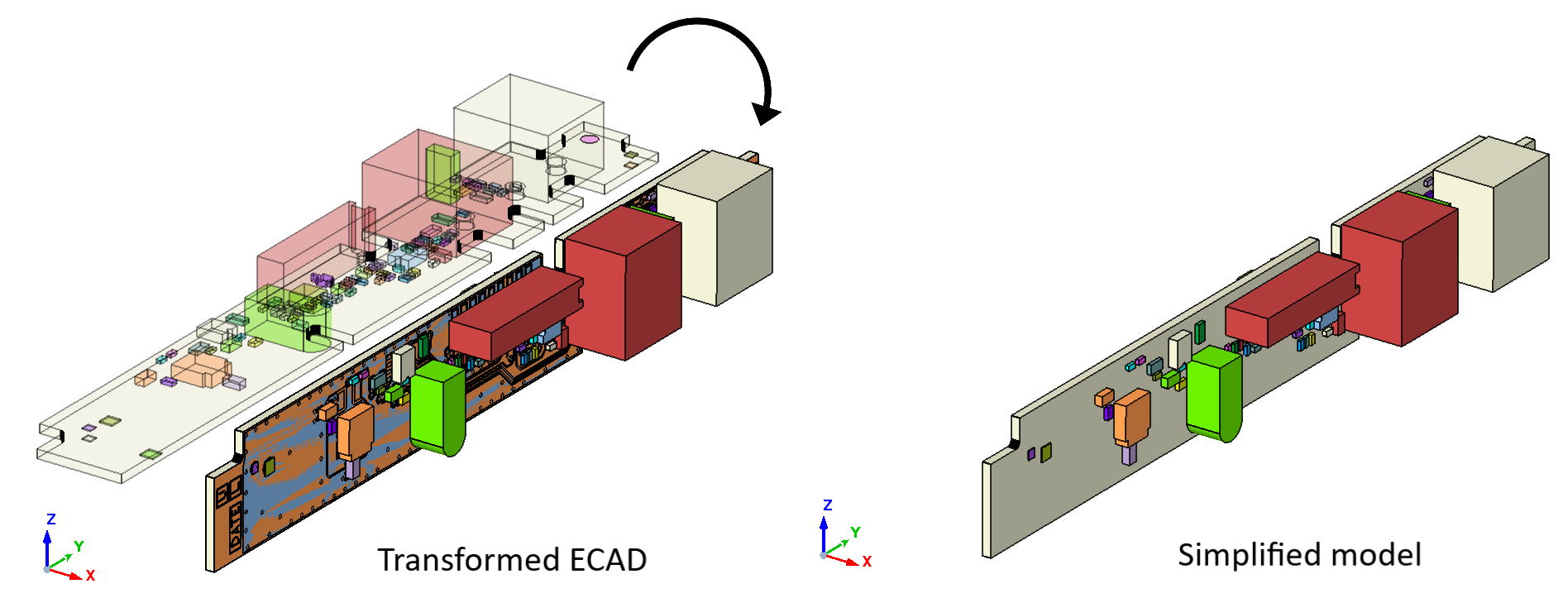
- In the case of a transformed ECAD model (where the thickness of the ECAD
model is not along the Z-Axis), metal content is computed according to its
orientation. However, the orthotropic material properties will be adjusted
to match its orientation only if the SIMLAB_TRANSFORM_MATERIAL_INFO
env is set to TRUE. Also, the simplified PCB will be created in the
respective orientation.
Homogeneous material approximation
Using "Create and assign equivalent material" a homogeneous equivalent PCB material can be created and assigned to the simplified PCB.
Layer Properties
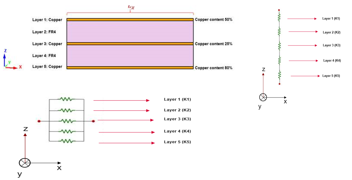
To compute any layer material parameters for any layer i, we can use rule of mixtures as follows:
Peffi = Pm * vm + Pd * vd
| Pm | Material parameter of metal |
| vm | Metal fraction |
| Pd | Material parameter of dielectric |
| vd | Dielectric fraction which is vd = 1 - vm |
Equivalent Properties
After computing the layer properties,the equivalent material parameters are computed by using the metal layout approach. The equivalent material properties can be approximated as either orthotropic or isotropic. The Isotropic material model can be used for fatigue analysis.
Orthotropic approximation
From the metal layout approach, the following relations are derived to compute the material parameters.
- Density
- Reference temperature = 295.15K
- Young's modulus (X,Y,Z) direction
- Poisson's ratio (XY,YZ,XZ) direction
- Shear modulus (XY,YZ,XZ) direction
- Thermal expansion (X,Y,Z) direction
- Thermal conductivity (X,Y,Z) direction
- Specific heat
- Electrical resistivity
- Temperature coefficient at resistance
Isotropic approximation
The effective or equivalent properties are found out by weighted average as follows:
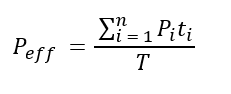
| Pi | Any material parameter say Young's modulus, density, thermal conductivity so on at Layer i |
| ti | Thickness at Layer i |
| T | Total thickness of PCB |
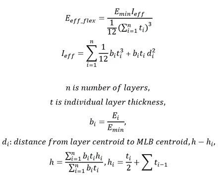
Bending modulus computation:
Equivalent bending modulus of the PCB can be calculated based on the given layer properties. Bending modulus is computed by following relation,
Manual entry of Layer information
If the selected model is not an ECAD model, SimLab allows to enter the data in tabular form and allows to create equivalent material from the entered data.
Export and Import:
- For ECAD models with PCB information, Export of PCB information in CSV file is supported.
- For Manual entry of PCB layer information, Import and Export of CSV file is supported.
Sample CSV file:LayerInformation.csv