TCP Pad
TCP component is tape carrier package. Check the specification of TCP component pad (pin).
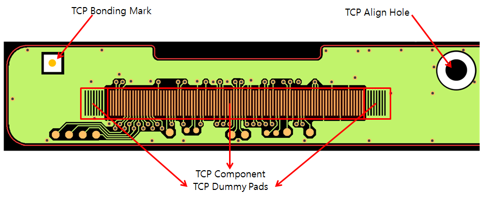
Figure 1.
- TCP Component Definition: Define target TCP component.
- Component Group Selection: Select target component from component group list.
- TCP Component Area: Define TCP component area.
- Auto-Detection of Dummy Pad: This menu is automatically detected the TCP pad in the defined area. If there is no component, TCP pad and dummy pad are recognized as TCP pad. If there is a component, it checks using the Expand checking area based on TCP component toward major axis condition.
- TCP Pad: Define a TCP pad area only with a TCP component.

Figure 2. - TCP Pad + Dummy Pad: Define a TCP pad area with a TCP component and
a dummy pad.

Figure 3. - Expand checking area based on TCP component toward major axis: If
there is a component other than a TCP pad or a dummy pad between TCP
pads in the defined area, this option is used to expand a checking
area by the given value from the center point of a TCP
component.
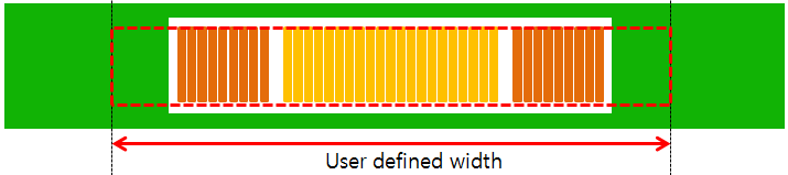
Figure 4.
- Hatching Existence Check Under TCP Component Area: Checks whether there is
hatching or not under the TCP component area.
- Inner Layers: Search hatching in inner layers, except top and bottom. If there is no hatching, it is a fail.
- Adjacent Layer: Search hatching on adjacent layer. If there is no hatching, it is a fail. If TCP component is placed on top, PollEx DFM searches second layer to find hatching.
- Component Clearance: Checks the clearance between the TCP component and
another component.
- Item: Specify the item name.
- Comp Group: Select component group.
- Clearance: Set the clearance value between TCP component and specified components.
- Measure Base: Select measure basement to be used for specified components.
- Remainder: Set the clearance value between TCP component and components, not defined in table.
- Exclude Checking for Selected Component Group: Select void-checking component group from the component group list.
- Checking
- Silkscreen Existence on Reverse Side of TCP Component: Check whether silkscreen is or is not on the reverse side of TCP component placed layer.
- Clearance between TCP Component and Vias: Set the clearance value
between TCP component and Vias.
- Measuring Base with TCP Component Area: TCP component measuring base will be TCP component area define at ②, TCP Component Area.
- Vias only Connected to TCP Component Pads: If this option is
checked, PollEx DFM checks
clearance only for Vias connected to TCP component pins.
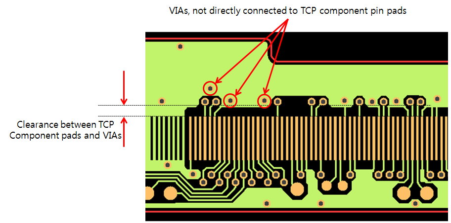
Figure 5.
- Clearance between TCP Component Pad and Copper-Pours: Set the clearance between the TCP component pad and copper-pours.
- Solder Mask Existence Checking in TCP Component Area: Checks if solder mask data is under TCP component area.
- Allow Patterns Connecting with Pads for One Way: If any pads are
connected in both direction, it is a fail.
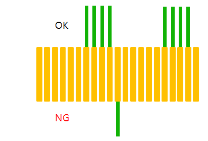
Figure 6. - Do not allow neighboring NC Pins: If there are neighboring NC pins, PollEx DFM detects them and defines them as a fail.
- Allow Patterns Connecting with Zigzag Style: For specified TCP
component pins, check if their pattern connection has a zigzag
connecting structure. If not, it fails.
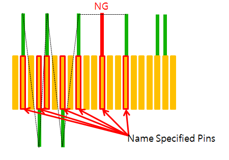
Figure 7.- Target Pins’ Name: Specify pins names in TCP component.
- TCP Pad Size
- Height: Enter a value to check the height of the TCP pad.
- Width: Enter a value to check the width of the TCP pad.