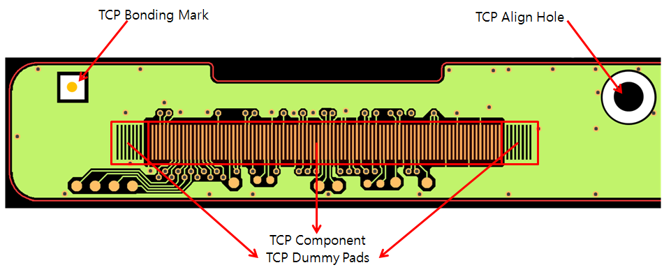
The TCP component is a tape carrier package. The TCP bonding mark is constructed with
solder mask and pad shape. Placed at the edge of the TCP component, the TCP bonding
mark is used to identify the TCP component.
The TCP Bonding Mark dialog contains the following
sections: Figure 1.
TCP Component Definition: Define the TCP components.
Component Selection: If components are registered as a group, select
them from list.
Minimum Pin Count Limit: Using this option, among components group,
you can choose target components which have more pins than the given
value.
TCP Bonding Mark Definition: Define TCP bonding marks.
Component Selection: If TCP bonding marks are registered as a
component, select them from component group list.
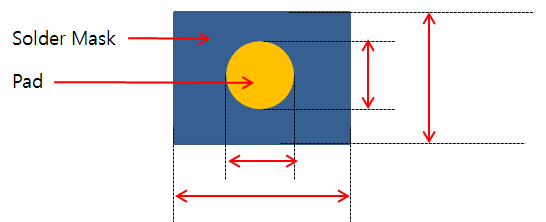
Board Figure: If TCP bonding marks are designed with board figure
geometries, specify their mark size and pad size.
Mark Size: Set the mark size X and Y.
Pad Size: Set the pad size X and Y.
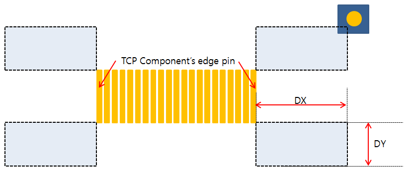
Mark Searching Area from Component’s Pin Edge: TCP bonding mark
should be placed near the TCP component. To define TCP bonding mark
finding area from TCP component edge pad, set DX and DY value.
Checking
Placement: Check the TCP bonding mark placed layer.
TCP Component Layer: When this option is checked, TCP
bonding mark should be placed at the same layer with TCP
components or it is a fail.
Top: Under this option, all TCP bonding marks should be
placed on the top.
Bottom: Under this option, all TCP bonding marks should be
placed on the bottom.
Check Difference between Two-sides Mark Shape: If this option is
checked, PollEx DFM checks the shape of
side TCP bonding mark. If the shape is different, it is fail. Figure 2.
TCP Bonding Marks’ Counting: To check the number of TCP bonding mark
on design, set the value and select maximum/minimum/matching
condition.
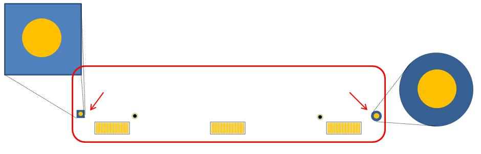
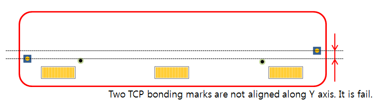
Arrangement for Y Location: Check side edge’s TCP bonding mark
alignments along Y-axis. Figure 3.
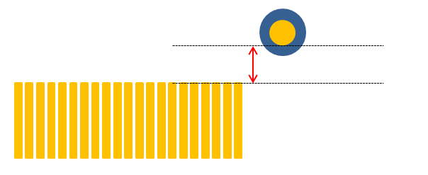
Y Axis Clearance between TCP Component and TCP Mark Pad’s Edge: Set
the Y-axis clearance value between TCP component and TCP bonding
mark pad edge. Figure 4.
Tolerance: If Y-axis values differences are within
tolerance, PollEx DFM defines them
as the same value.
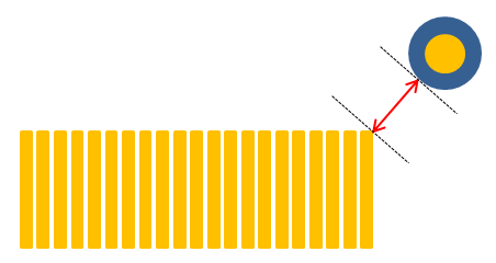
Clearance between TCP Mark and Components: Set the clearance value
between TCP bonding mark and TCP component. Figure 5.
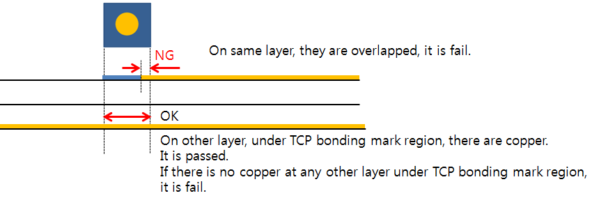
Copper Existence: Check TCP bonding marks are overlapped with
copper-pour on the same layer and copper-pour existence under TCP
bonding mark region on other layer. Figure 6.
Silkscreen Overlapping: Checks TCP bonding marks overlapping with
silkscreen data.
Gerber: To get silkscreen screen, use GERBER file data. Use
this option after reading GERBER file for top and bottom.
Top: Select GERBER top layer from layer list.
Bottom: Select GERBER bottom layer from layer
list.
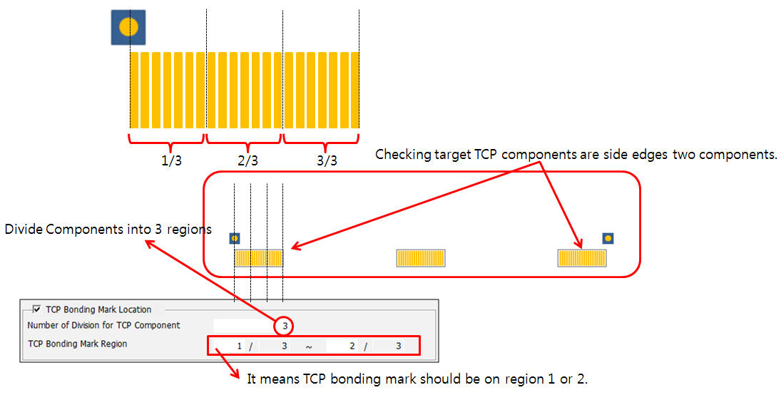
TCP Bonding Mark Location: Check the TCP bonding marks location for
TCP components at edge of board. Figure 7.
Number of Division for TCP Component: Set value to divide
component region.
TCP Bonding Mark Region: Set region on which TCP bonding
marks should be placed.