Placement at Reverse Side
Verify if components are viable for reverse placement on the same board layer.
BGA or CSP-type components are weak to stress, so you must avoid placement on the reverse side of these fragile components.
More detailed information:
- Except for SMD Pins, not having Metal-Mask: Exclude SMD Pins that do not have a metal mask from analysis.
- Item: Specify the name of an item.
- Component Group: Specify the component for analysis. For example, BGA, or CSP-type components.
- Check Base: Select a measurement base.
- Measure (**The issue of unclear criteria for Vertical and Horizontal orientation arises when applying Pad Shape to components other than Shield Can. Therefore, Pad Shape is exclusively applied to Shield Can.)
- Expand Area: Set the clearance area.
- Horizontal: Set the clearance horizontal area.
- Vertical: Set the clearance vertical area.
- Reverse Side Component Group: Specify the component that is prohibited from placement on the reverse side of the analyzed component.
- Reverse Component Check Base: Select a measurement base. (**Among the Measure Base options, Pad Shape is unavailable.)
- Check Distance: Specify the distance for analysis.
Figure 1. Placement at Reverse Side Example 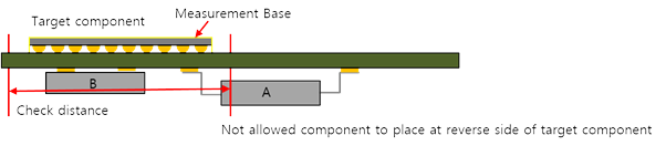
- Inner: Allowed if components placed on the reverse side within the target component's measure base area.
- Boundary: Allowed if components placed on the reverse side are overlapped with the target component's measure base.