Export to 3D Format
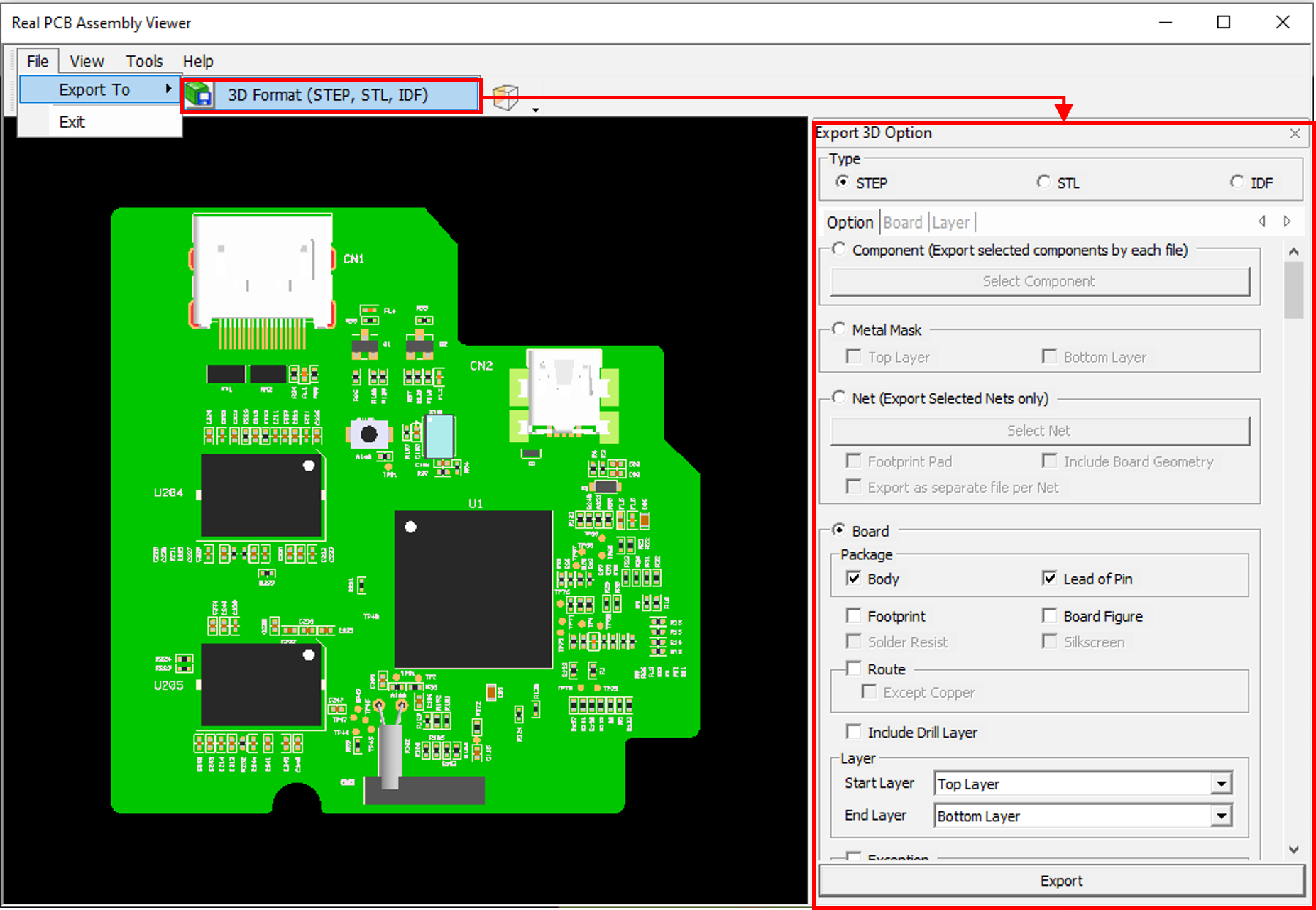
- Type: Specify the 3D data type to export.
- Option: Set options for exporting as 3D data.
- Component (Export selected components by each file): Option to export the
selected components used in the design data with 3D shape.
Figure 2. 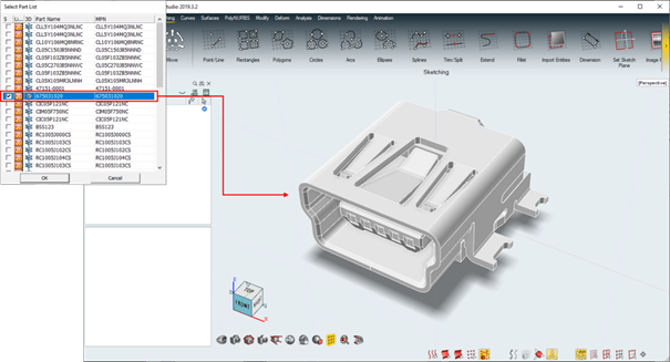
- Metal Mask: Metal Mask drawn as positive on the PCB design data is converted
into negative and exported as 3D data. You should set the Metal Mask thickness
in the layer setting.
Figure 3. 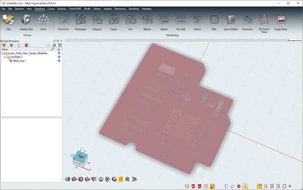
- Net (Export Selected Nets only): Option to export the selected Net as 3D
data.
- Footprint Pad: Export including the footprint pad which connected to the net.
- Include Board Geometry: Export including the PCB board shape.
- Export as separate file per Net: Export a separate file per a net.
Figure 4. 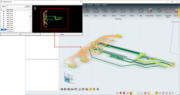
- Board: Option to export the shapes of the board and components in the design
data.
Figure 5. 
- Package: Select whether to export package Body and Lead of Pin.
- Footprint: Select whether to export part footprint.
- Board Figure: Select whether to export the board figure drawing in the PDB design data.
- Solder Resist: Select whether to export the solder resist.
- Silkscreen: Select whether to export the silkscreen.
- Route: Select whether to export the routing.
- Except Copper: Option to exclude the copper-pour.
- Include Drill Layer: Select whether to export the shape of drill properties like through hole, via hole and figure hole.
- Layer: Set the range of layers to be exported.
- Start Layer: Set the start layer.
- End Layer: Set the end layer.
- Exception: Option to exclude components and nets.
- Component: Select the components to be excluded from the list or use the Component DB (*.txt) file.
- Net: Select the nets to be excluded from the list.
- Board: Select the board to export from the list if there are multiple boards in the PCB design data like the Panel PCB.
- Layer: Set the thickness of the PCB board.
- Table
- No.: Display the physical layer number.
- Name: Display the layer name.
- Thickness(mm): Display the thickness of the layer. The displayed value can be modified by double-clicking it.
- Board Total thickness(mm): If checked this option, the thickness of layers specified above is ignored and user can define the total thickness of the board.
- Solder thickness (mm): Set the thickness of the solder resist.
- Silk thickness (mm): Set the thickness of the silk.
- Metal thickness (mm): Set the thickness of the metal mask.
- Export: Set the export path.
- View
- Component
- General View: Display only PCB shape except 3D components.
- PCB Assembled View: Display both PCB shape and 3D components.
- Toggle On/Off: Select whether to display per component reference in the list.
- Lead On/Off: Select whether to display the component lead.
- Board Outline: Option to turn on or off the board outline display, only when the width value is drawn more than 0.
- Route: Option to turn on or off the 3D PCB geometry.
Figure 6. 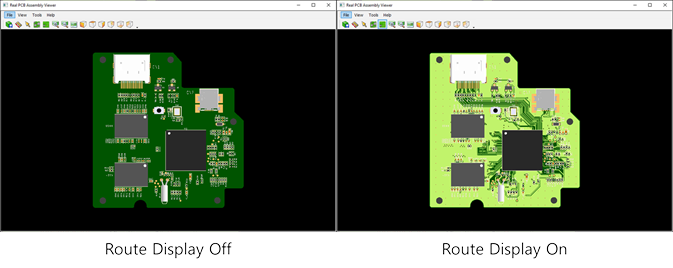
- Silk: Option to turn on or off the display of Silk Screen.
- Solder Resist: The solder mask designed as positive in PCB design data is
converted to negative to display the solder resist layer as much as the input
thickness.
Figure 7. 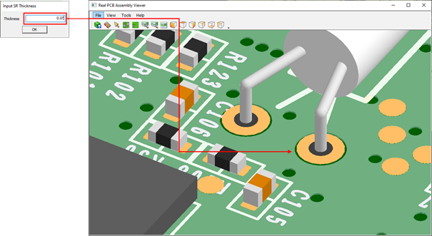
- Constrain Axis: Option to limit the rotation axis.
- Toggle Axis Cross: Option to turn on or off the display of XYZ axis pivot.
Figure 8. 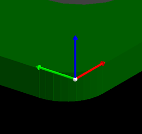
- Zoom In/Out: Option to zoom in or out.
- Zoom 1:1: Restore the display to default.
- Switch Variant: Option to view the imported variant board.
- Select the variant board to check the status of the variants.
- View Variant Lists: Review the variant lists and comparison between variants.
- Color Setting: Specify the color of each layer.
Figure 9. 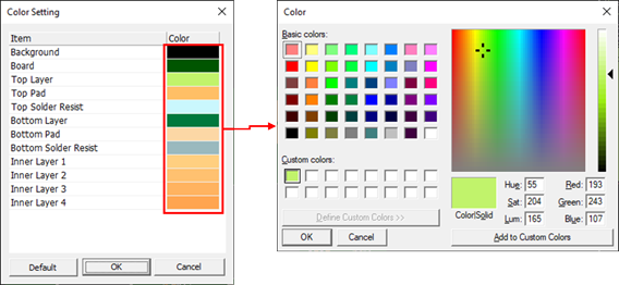
- Tools: This item provides convenient functions such as measuring distance between parts and cutting board view.
- Component List: Search the parts used in the design.
Figure 10. 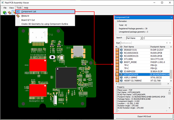
- Export information of components in the PCB design.
- Total: The total number of components used in the PCB design.
- Registered package geometry: The number of components with the 3D geometry registered in the UPE library.
- Unregistered package geometry: The number of components with the 3D geometry not registered in the UPE library.
- Search: Search components by Part Name or Reference Name.
- Part/Reference Table: List of components used in the PCB design can be checked
the information. The component is highlighted in red when selected a component
from the list. Check the property information of selected component.
Figure 11. 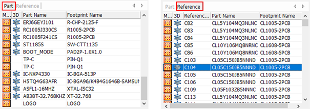
- Measure: This menu measures the distance between components.
Figure 12. 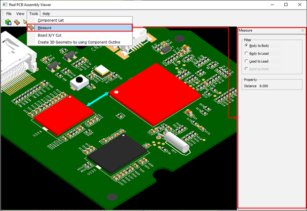
- Body to Body: Measure the closest distance between the bodies. The measured value can be checked in Property.
- Body to Lead: Measure the closest distance between the body and lead. The measured value can be checked in Property.
- Lead to Lead: Measure the closest distance between the leads. The measured value can be checked in Property.
- Board X/Y Cut: Check the PCB cutting surface.
Figure 13. 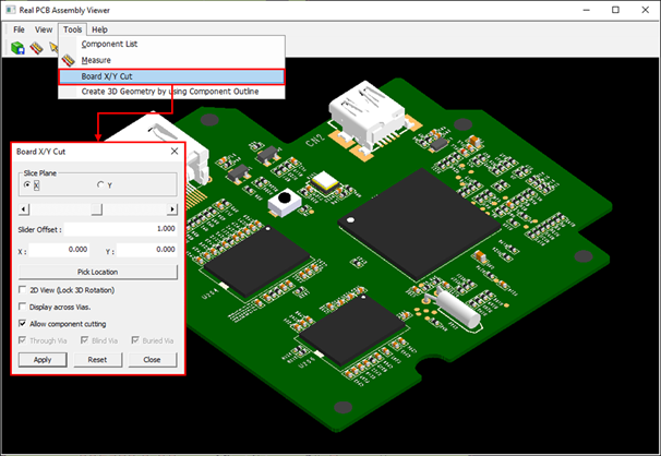
- Slice Plane: Select the X or Y axis of the cut plane.
Figure 14. 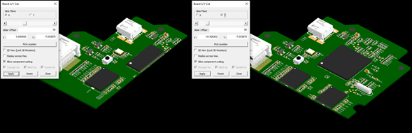
- Scroll: Move the selected cutting plane by moving the slider scroll.
Figure 15. 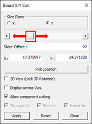
- Slider Offset: Slide bar moves by the Slider Offset value.
- X, Y: Indicate the X, Y coordinates of the cutting plane.
- Pick Location: Specify the cutting plane location by clicking the desired location.
- 2D View (Lock 3D Rotation): Display the cutting surface in 2D.
- Display across Vias: Select whether to display Vias in the cutting plane.
- Allow component cutting: Select whether to cut the component.
- Through Via, Blind Via, Buried Via: Select whether to display per via type.
- Create 3D Geometry by using Component Outline: 3D geometry is created by using
the COC shape and height information of the component if there is no 3D UPF
library.
Figure 16. 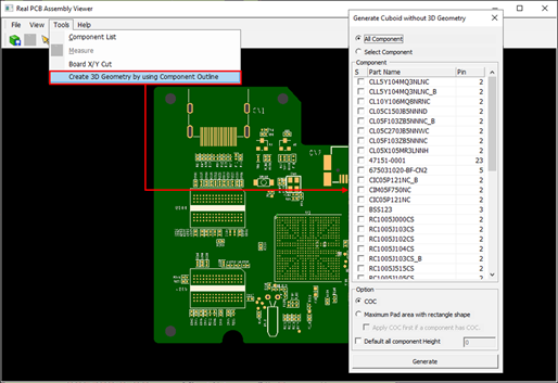
- All Component: Generate 3D geometry for all components in the PCB.
- Select Component: Generate 3D geometry for the selected components from the list.
- Option: Option to generate 3D part shape.
- COC: 3D part shape is created based on the component boundary of the footprint.
- Maximum Pad area with rectangle shape: 3D part shape is created based on the largest rectangular area of the footprint pad.
- Apply COC first if a component has COC.: If a part has a COC (component boundary), 3D part shape is created based on the component boundary of the footprint first. The rest parts which do not have the COC will be created the 3D part shape based on the largest rectangular area of the footprint pad.
- Default all component Height: 3D part shape is created the height of all parts with the entered value.