SS-V: 9001 Wave Reflection on Dielectric Boundary
Test No. VE02Propagation of the fundamental mode wave in a waveguide and reflection from dielectric boundary
Definition
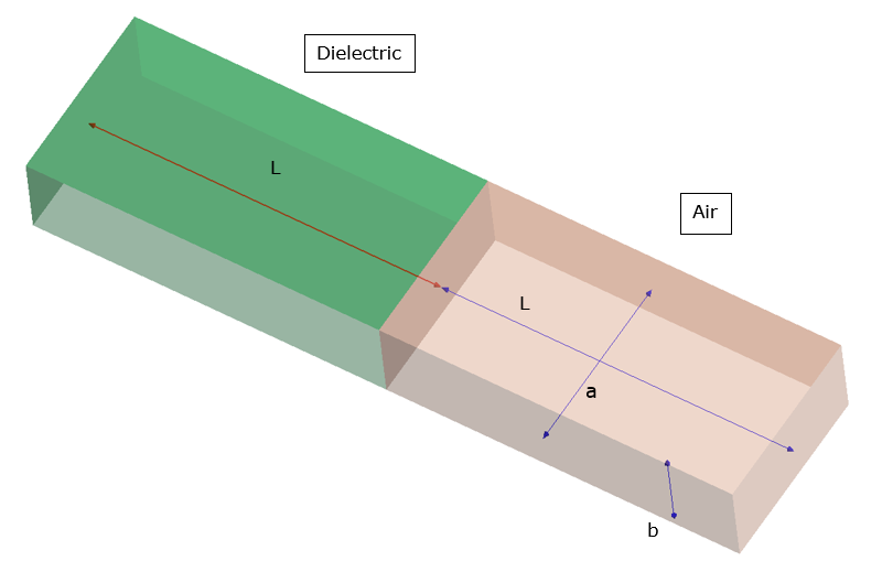
- Figure 1: a = 20mm, b = 10 mm, L = 40 mm
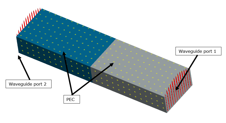
- Side walls are at the PEC (Perfect Electric Conductor) conditions and ports are at the end faces
- Properties
- Value
- Dielectric relative permittivity
- 4.0
- Dielectric relative permeability
- 1.0
- Air relative permeability
- 1.0
- Air relative permeability
- 1.0
Results
| Parameter | Frequency (GHz) | Theory | SimSolid | % Difference |
|---|---|---|---|---|
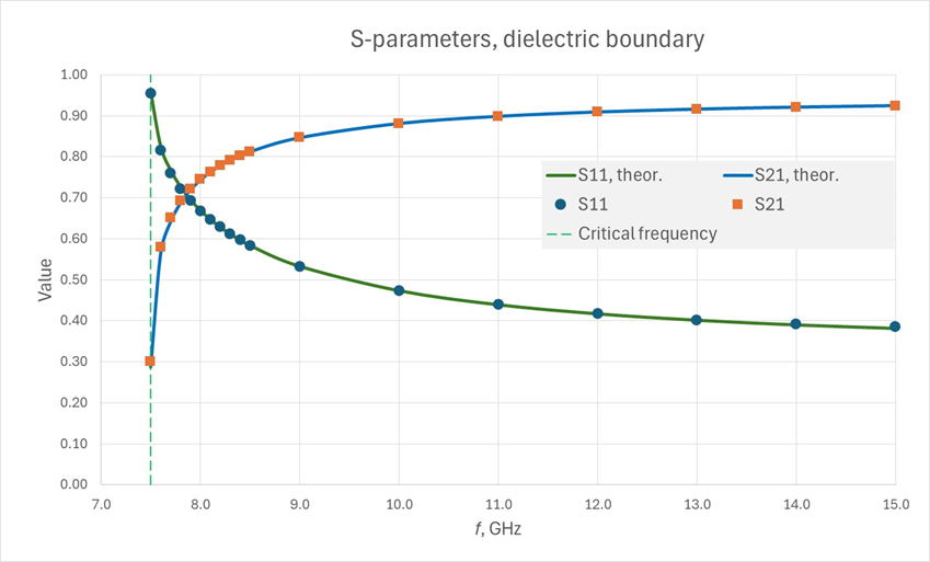
| S11 | 7.5 | 0.95 | 0.96 | -0.4 |
| 7.6 | 0.82 | 0.83 | -1.2 | |
| 7.7 | 0.76 | 0.77 | -1.0 | |
| 7.8 | 0.72 | 0.73 | -0.7 | |
| 7.9 | 0.69 | 0.70 | -0.4 | |
| 8.0 | 0.67 | 0.67 | -0.2 | |
| 8.1 | 0.65 | 0.65 | -0.08 | |
| 8.2 | 0.63 | 0.63 | -0.01 | |
| 8.3 | 0.61 | 0.61 | -0.01 | |
| 8.4 | 0.60 | 0.60 | -0.02 | |
| 8.5 | 0.58 | 0.58 | -0.06 | |
| 9.0 | 0.53 | 0.53 | -0.2 | |
| 10.0 | 0.47 | 0.47 | -0.03 | |
| 11.0 | 0.44 | 0.44 | 0.1 | |
| 12.0 | 0.42 | 0.42 | -0.06 | |
| 13.0 | 0.40 | 0.40 | -0.1 | |
| 14.0 | 0.39 | 0.39 | 0.4 | |
| 15.0 | 0.38 | 0.38 | 0.8 |
| Parameter | Frequency (GHz) | Theory | SimSolid | % Difference |
|---|---|---|---|---|
| S11 | 7.5 | 0.29 | 0.30 | 4.8 |
| 7.6 | 0.56 | 0.58 | 2.6 | |
| 7.7 | 0.64 | 0.65 | 1.5 | |
| 7.8 | 0.69 | 0.69 | 0.8 | |
| 7.9 | 0.72 | 0.72 | 0.4 | |
| 8.0 | 0.74 | 0.74 | 0.2 | |
| 8.1 | 0.76 | 0.76 | 0.06 | |
| 8.2 | 0.78 | 0.78 | 0.01 | |
| 8.3 | 0.79 | 0.79 | -0.003 | |
| 8.4 | 0.80 | 0.80 | 0.01 | |
| 8.5 | 0.81 | 0.81 | 0.03 | |
| 9.0 | 0.85 | 0.85 | 0.09 | |
| 10.0 | 0.88 | 0.88 | 0.01 | |
| 11.0 | 0.90 | 0.90 | -0.03 | |
| 12.0 | 0.91 | 0.91 | 0.01 | |
| 13.0 | 0.92 | 0.92 | 0.03 | |
| 14.0 | 0.92 | 0.92 | -0.07 | |
| 15.0 | 0.92 | 0.92 | -0.1 |
1 Pozar, D.M., Microwave
Engineering, 4th Edition, John Wiley & Sons, Inc., 2012, 4.1.