Power-Width
This DFE rule checks routed pattern trace widths compared to specified minimum and maximum widths.
One of the most common causes of voltage drop failure in power delivery is the resistance associated with the power (VBUS) trace. While budgeting for voltage drop, you must consider the trace length, maximum current being supplied for normal operation, and total resistance associated with the power trace.
The absolute minimum power trace width must be determined by the amount of current it has to carry.
- Item: Enter item name.
- Net: Select a power net group.
- Object: Define test object.
- Start Component: DFE checks pattern width between the start component and the end component only.
- End Component: DFE checks pattern width between the start component and the end component only.
- Limit: Select a width check type – minimum/maximum/range.
- Segment Width: Assign width criteria for individual segments.
- Tolerance Type: Assign allowable width tolerance type (Value/Ratio).
- Tolerance: Assign allowable width value/ratio.
- Pin Escape: Enter a radius of circular region around pins to be excluded for the rule check.
- Inner Only: DFE checks inner layers only.
- Component Keep IN/OUT: Define test region. For example, you can test inside
or outside the breakout region of CPU with different test
values.
- Component Keep in/out:
- Component Group: Select required component group which is used for defining the test region.
- Region: Define the required test region.
- IN: Test inside of the breakout region of target component.
- OUT: Test outside of the breakout region of target component.
- Range (COC+distance): Enter the distance value to define breakout range. The COC (Component Overlap Check) plus this distance value is considered the test range.
- Target Layer: Select the required test layer.
- All Layer: Test all layers.
- Component Place Layer: Test only component placement layer.
- Exclude Fill Area: The copper fill to be excluded for this rule checking.
- Composite Power Net: DFE uses composited power net instead of single power
net.
- Composite Power Net
- Passive Comp: The DFE makes composite net that are connected through this passive component.
- Exception Net: Nets that should not be merged into composite net.
- Composite Power Net
- Inadequate power supply rating.
- Excessively long system power supply cable harness.
- Poor system power supply load regulation.
- Underrated over current protection device.
- Inadequate Power Trace Width.
- Overly resistive ferrite beads.
- Inadequate wire gauge for VBUS and GND in the harness of the USB port assembly.
IR-Drops
Voltage that develops across a conductor as a result of its electrical resistance.
This voltage is proportional to the current that flows though the conductor (V = IR).
Results in a drop-in voltage available at the load devices (Vload = Vsupply – Vdrop).
The problem is made worse by the lower operating voltages common in core power supplies today.

Figure 1.
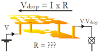
Figure 2.
In some cases, power trace width and clearance rules are contradicting between manufacturing concerns and electrical performance concerns. Therefore, DFM and DFE rules must be considered at the same time.
Determine Minimum Trace Width Requirement

Figure 3.
Since the maximum allowable current for a PCB pattern is 1,000 mA/mm, power pattern should be bigger than 0.5 mm to flow 500 mA and it can be calculated as:
1,000 mA: 1 mm = 500 mA: X
X = 1mm * 500 mA / 1,000 mA = 0.5 mm