Decap
This rule checks for the number of capacitors per each PWR/GND pin to help the designer to determine the stability of IC component’s power supply. The rule also reports the distance between capacitor and IC components.
Voltage regulator adjusts the amount of current it is supplying to keep the output voltage constant but can only effectively maintain the output voltage for events at frequencies from DC to a few hundred kHz or low MHz.
At higher frequencies, Decap works as a device’s local energy storage and the stored energy can respond very quickly to changing current demands.
In order to effectively maintain the output voltage at high frequency, it is ideal to supply power to pins through DECAPs.
- Minimum Number of Total Decap: Enter a required minimum number of capacitors on whole PCB.
- Item: Enter item name.
- Power Net: Select a power net group.
- GND Net: Select a ground net group.
- Decap Comp: Select a capacitor component group.
- Comp: Select a target IC net group that needs decoupling capacitors.
- Distance: Assign a distance within which decoupling capacitors should be placed from IC components.
- Pin Type: Specify pin type for check. (Power Pin/Power+GND)
- Power Pin: Checks decap count of every power pin.
- Power + GND Pin: Checks decap count of every power pin and ground pin.
- Count: Required capacitor minimum count.
- Decoupling Capacitor (Decap) This capacitor is connected to the IC component’s power pin. At the time of a sudden surge of power consumption or during rising/falling time, it supplies a stable power to IC components. It is used mainly in high speed signal circuits.
- Bypass Capacitor This capacitor is used to reduce power noise. A bigger
capacitance capacitor is used for lower frequencies. A smaller capacitance
capacitor is used for higher frequencies.
Figure 1. 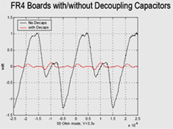
Figure 2. 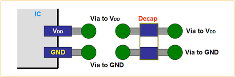
Decoupling Capacitor Usage on Multi-Layer Board
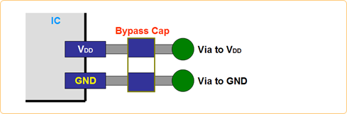
Bypass Capacitor Usage on Multi-Layer Board
- Advantage: Lower number of capacitors is required since some VDD-GND pairs can share one capacitor.
- Disadvantage: Larger current loops compared to pin-decoupling.
Provide at least half as many capacitors of the same value as there are supply pairs at your microcontroller.
Avoid long traces between MC pad and via to supply plane (additional inductance).
Provide two vias in parallel if possible.
Best decoupling concept is a combination of local and global decoupling. This brings some more costs for discrete components but can save development time and redesign activities at critical applications.