Net Topology Analysis
Net Topology Analysis integrated into the radiated emission provides the feature of Adding Virtual Termination (such as passive component, ground, and DC Source) in front of the IC model (Drivers and Receivers). Therefore, the user can do a what-if-simulation from the radiated emission perspective.
Net Topology Analysis is a valuable tool for creating or visualizing detailed physical network structures in schematic form, enabling signal integrity analysis on the interconnection in a PCB system. During the pre-routing stage, it can be effectively employed to explore various network configurations, identifying constraints for critical connections.
With the assistance of the Net Topology Analyzer, PCB designers and SI engineers can sketch out optimized signaling patterns for specific or critical connections that handle very weak signals or operate at extremely high speeds. Careful consideration of routing layout and termination techniques is essential for analog and high-speed digital signals, such as clocks, to ensure signals transmit correctly. Depending on the number of loaded ICs and the length of routing, using termination may become unavoidable. The AC/DC characteristics of driver ICs are also a key factor influencing signal quality in PCB systems, making it crucial for SI analysis to address these aspects.
When you select the dialog will display. Then if you choose the object you want to analyze using the Select Net button, the Analyze Net Topology is activated as below.
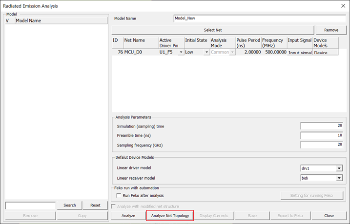
Figure 1.
Users can select only 5 different types of components (highlighted in red in the manual bar section) and add these components to both the Driver and Receiver sides.
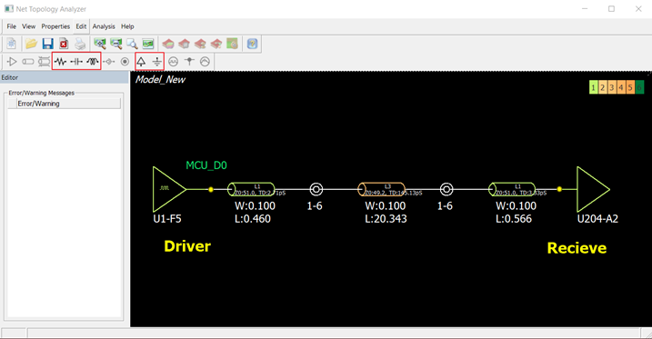 Figure 2.
 If you add components between the transmission line or via models, it may affect the simulation results with a faulty. So add the components at the yellow dot pointed in the figure.
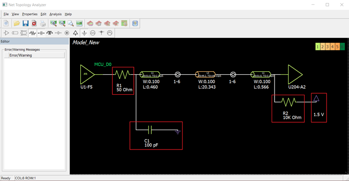
Figure 3.

Figure 4.
In the Radiated Emission Analysis dialog, the Analyze with modified net structure checkbox becomes active (marked in red box). This allows you to perform radiated emission analysis with the modified net topology. You can write a suitable name in the Model Name section for saving and managing the model.

Figure 5.
After the simulation, click Save button in the Radiated Emission Analysis dialog box. This stores the modified net topology file (*.ntfb) in the Radiation folder within the *.pdbb directory where the user has modeled.

Figure 6.

Figure 7.

Figure 8.