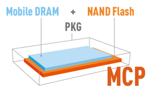
MCP Analysis
Multi-Chip Package (MCP) is a semiconductor packaging technology that combines multiple chips into one package, which can save space and cost while improving functionality and performance.
MCP is used in various fields. For example, in mobile devices, MCP consolidates chips into one place, saving space and reducing power consumption. One common application of MCP is in memory modules, where multiple memory chips are combined into a single package. In this case, the MCP can be used in place of other memory technologies like eMMC (embedded MultiMediaCard) or DIMM (Dual In-Line Memory Module). In the automotive industry, MCP integrates useful features such as safety devices and communication functions, providing many functions in a small space.
Features and Menu Description
The MCP simulation function allows users to evaluate the electrical performance and reliability of an MCP in a specific application. By simulating the MCP's behavior under different operating conditions, engineers can optimize the design, minimize signal integrity issues, and reduce the risk of failure.
- Electrical Board Description (EBD) file: This file describes the physical layout and interconnects of the PCB that the MCP will be mounted on. The EBD file is used to simulate the electrical behavior of the MCP in the context of the entire system.
- IBIS files: These files provide detailed information about the MCP's input/output (I/O) buffers, including the voltage levels, current drive strength, and timing characteristics.
- Pin Parasitic file: This file provides information about the MCP's package pins, such as the pin capacitance, inductance, and resistance. Pin Parasitic files are used to model the parasitic effects of the package pins, which can impact the MCP's performance.
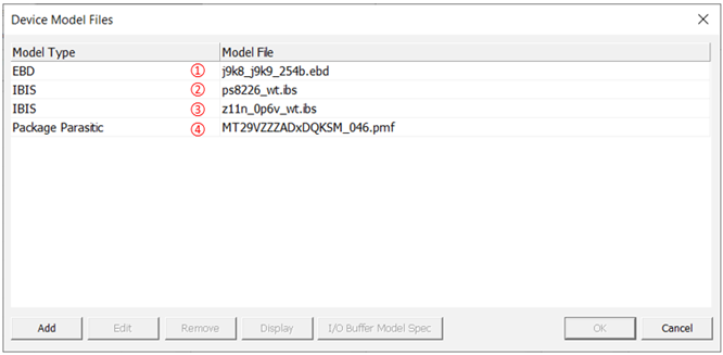
Through the Electrical & Thermal Properties menu, users can set up an EBD model and load the *.ebd, *.ibs, and *.pmf files from the Device Model Files dialog as below figure. Please note that the three files must be in the same directory for them to be imported automatically. To perform simulation using this model, *.ebd and *.ibs files must be in the same directory.
- EBD file: The EBD file is an IBIS Electrical Board Description. An EBD file
is a model of a PCB used for simulations. This file describes the electrical
characteristics of the pins and traces on the PCB. An EBD file used in
conjunction with IBIS models of the controller and memories can be used to
create a model of a module.
All inductance and capacitance parameters listed in the file are derived with respect to the defined reference planes within the board.
-
IBIS file for controller: This is an example file on the eMMC controller bare die component (PS8226) defined in the IBIS file ps8226_wt.ibs.
-
IBIS file for memories: This is an example of the memory IBIS model designed in the MCP. In this case, the memory consists of the same four dies. D1, D2, D3, D4 are the LPDDR4 bare die component (MT53D512M16D1Z11N) defined in IBIS file z11n_0p6v_wt.ibs.
-
Package Parasitic file: Files with package parametric information in the MCP.
After selecting *.pmf in the Device Model Files menu and clicking Display, you can see the Package Pin Parasitic Modeler dialog. Users can check the parasitic information for each pin, which is described in the [Path Description] section inside the *.ebd file.
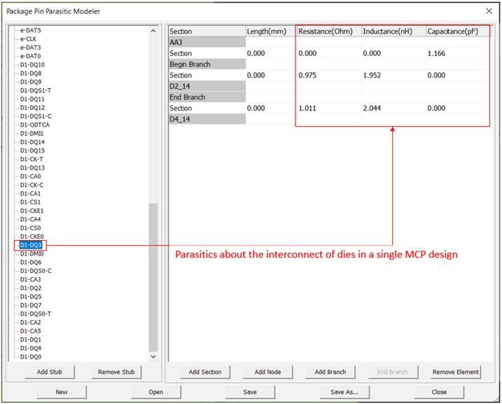
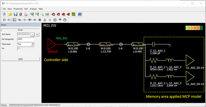
After completing the basic setup and opening the Net Topology Analyzer dialog, users can see the circuit configuration of the Controller side and the Memory area where the MCP model is applied. Users can confirm the pin package parasitic values in the model marked with yellow dotted lines. The figure below shows the MCP simulation model reflected with the parasitics of [Path Description] D1-DQ3 as indicated in the Package Pin Parasitic Modeler above.
Waveform Analysis
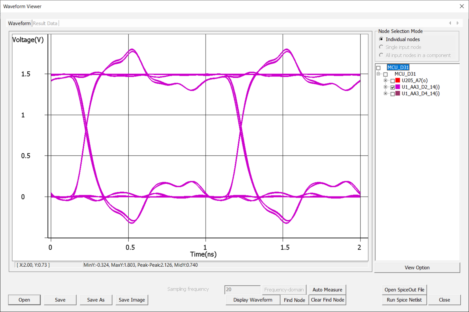
Waveform analysis is a simulation technique that involves running a transient circuit simulation on a network model for a specified amount of time. This process helps to generate time-domain voltage waveforms at both input and output nodes. After completing the analysis, the waveforms are displayed, and users have access to a range of measurement and display options in the waveform viewer. The waveform viewer provides a comprehensive overview of the behavior of the simulation model.
The following is the waveform result of the T-branch line with the MCP model applied, as described in the Features and Menu Description earlier.

Eye Diagram Analysis
To analyze a circuit using Eye Diagrams, a simulation is performed on the circuit model to obtain waveforms at the input nodes. These waveforms are generated by randomly selecting high/low states for the input signals of the net and adjacent nets. By overlapping multiple waveforms at the receiver node, an eye diagram is created. The analysis can be customized by modifying parameters such as the number of random pulses and bit pattern style before running the analysis.
The given diagram shows the output of an electronic T-shaped circuit with a specific MCP applied to it. The diagram represents the signal quality and helps analyze the circuit's performance in terms of data transmission.