Introduction
Signal integrity (SI) is a measure of the quality of an electrical signal.
In digital electronics, a stream of binary values is represented by a voltage (or current) waveform. Over short distance and at low bit rates, a simple conductor can transmit this width enough fidelity. However, at high bit rates and over longer distances, various effects can degrade the electrical signal to the point where errors occur, and the system or device fails. The purpose of the signal integrity tool is to analyze and mitigate these impairments.
Signal Integrity Analysis menus allow you to validate the design decisions throughout the design process including the selection of parts, materials, and board layer stack-up, placing components on the board, and routing signal and power/ground nets.
Previously, the switching rise/fall time of the devices in the components were much larger than the delays of the interconnections among components. As semiconductor technology brings in ever increasing speed, the device switching rise/fall times become smaller and smaller. When the rise/fall time of devices gets close to or smaller than the delay of interconnections, the integrity of the signals gets degraded. This phenomenon is called the transmission line induced signal degradation or signal integrity problem. In transmission line-based modeling, we need to model the time-of-flight delay of the interconnection much more rigorously than the standard lumped circuit analysis. This extra effort is necessary to account for the electromagnetic field interactions of the transmitted signals as well as time-of-flight delays among the adjacent wires. In the modeling process, the capacitive and inductive coupling among wires must be calculated. Furthermore, the impact of per-unit-length voltage and current changes in time need to be studied.
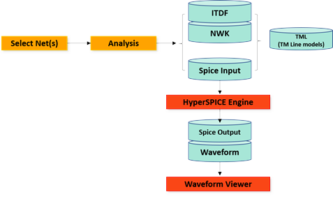
Figure 1.
Major Capabilities
- Extracting frequency dependent network parameters (S, Y, Z) and parasitic SPICE models in the forms of capacitance, inductance, resistance, and conductance for PCB interconnects configured with strip/micro-strip lines and vias.
- Transmission Line Analysis enables to get optimal physical dimensions of PCB interconnects (single-ended, differential pair) with designated stack up condition having desired electrical characteristics, for example: characteristic impedance, R, L, C, G, delay/unit length, velocity, attenuation, and skin depth, and so on.
- Signaling waveforms travelling among IC driver and receivers of the selected nets can be automatically displayed which reflects the effect of net topology, driver’s DC/AC characteristics, bias, and termination strategies. Signal delay, inductive/capacitive coupling and reflection phenomena are accounted for getting the travelling waveforms.
- Eye-diagram representing the quality of signal transmission can be extracted depending on the bit (pulse) shape and big generating algorithms (Random, ABS and PRBS)
- Topology editor provides the flexible and convenient ways to develop net routing topologies for certain critical nets, for example: high-speed clock and small analog signal as of in type of single-ended, differential, multi-coupled and system-level. (signal nets running multiple PCBs)