Environment Setting
In this section, PollEx Environment setting methods are explained.
From the menu bar, click to open the Environment dialog. Select General from the navigation tree window.
Default File Path

Figure 1.
- Default net class file path: The net class file will be used to group DDR bus nets according to their electrical characteristics.
- Default material file path: you can set default material file path. This file contains parameter information for all materials that make up the PCB.
- Default MPN reference file path: you can set default MPN reference excel file path. This file contains information that matches MPN and CPN.
- Default part library directory: you can set default UPF directory path. The UPF contains electrical libraries such as footprints, logical symbols, 3 dimensional shapes, data sheets, simulation model, mount data for electrical/thermal analysis.
Linear Model
Select Analysis to set the linear device model file path.

Figure 2.
IO buffer device models of input and output pins of signal nets are stored in the part data file of individual components. When the device models are not available in the part data, the default device models defined here are used for transient simulation of signal integrity analyses. With the use of Linear Device Modeler, users can create linear output (driver) and input (receiver) device models and store them in a linear device model file. PollEx SI provides you with a system default linear device model file, UDVS.dmf.

Figure 3.
Allowable Minimum Trace Width

Figure 4.
During Transmission Line Analysis, you can let the program find the trace widths whose characteristic impedance values match the target impedance values by selecting the Get Impedance Matching Trace menu.
- Core layer trace min width: Minimum trace width of PCB limited by PCB manufacturer (Outer Layer)
- Microvia layer trace min width: Minimum trace width of PCB limited by PCB manufacturer (Inner Layer)
Default String for Differential Pair Net Pairing
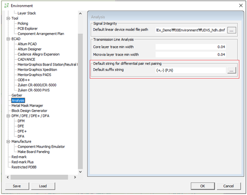
Figure 5.

Figure 6.