Radiated Emission Analysis Dialog
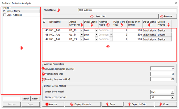
Figure 1.
- Model Name: Assign Model Name.
- Select Net: Nets for analysis can be selected over Select
Net dialog.
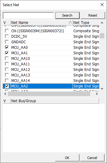
Figure 2. - Remove: Remove selected net from Net List Window.
- Active Driver Pin: You can specify the active driver pin among the connected pin to this net. The other pins will be assigned as receiver pin(s) automatically.
- Initial State: You can specify the initial value of input waveform.
- Analysis Mode: You can select the signal to assert the mode of the differential pair net. (Differential Mode/Common Mode)
- Pulse Period(ns): You can adjust the driver’s operating frequency/speed by changing this value. The default pulse period of input signal is automatically obtained from the operating frequency information of the net.
- Input Signal: The Input Signal dialog opens. You can review and change the
detailed parameters which can specify the actual shape of the input signal,
for example: TD (Time Delay), TR (Rise Time), TR (Fall Time), PW (Pulse
Width), and pulse train.
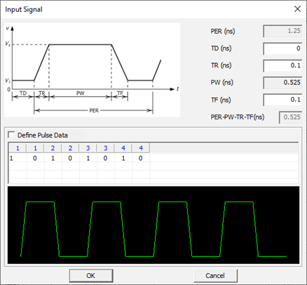
Figure 3. - Device Models: The Device Model List dialog will be open. You can review
default device models selected for the output and inputs pins. For the
selected active driver, actual driver model can be selectable among many
different models in IBIS or Linear device model types. You can use one of
available models considering the output impedance, driving capability
measured by output current level and operating frequencies.
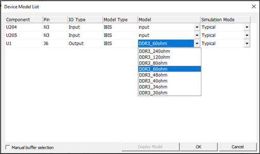
Figure 4. - Net List Window: All the selected nets are displayed in this window.
- Simulation (sampling) time (ns): You can edit end time of the SPICE transient analysis.
- Preamble Time (ns): Simulation start after this time to wait until status of internal circuit becomes stable.
- Sampling frequency (GHz): Adjust the sampling frequency point for FFT. The sampling time intervals is 1/(sampling frequency).
- Analyze: Simulation starts.
- Display Currents: The Display Current dialog opens. You
can review the simulation result in this dialog.
- Save: Any simulated nets can be saved and selected again when the
PCB reactivated later by clicking Copy. The saved models are listed
in the left-hand side of the dialog. You can select the saved models
anytime and copy the model to view the model, view the analysis
results, edit the model, and rerun analysis.
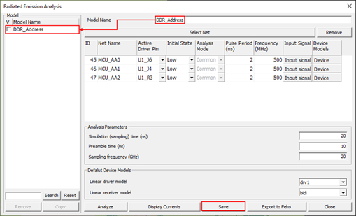
Figure 5. - Export to Feko: the simulation result will be exported in XML format file. This file is saved in Radiation/Model_Name directory under the PCB design job folder. The model name plus .REI is used for the file name.
- Save: Any simulated nets can be saved and selected again when the
PCB reactivated later by clicking Copy. The saved models are listed
in the left-hand side of the dialog. You can select the saved models
anytime and copy the model to view the model, view the analysis
results, edit the model, and rerun analysis.
- Close: Close the Radiated Emission Analysis dialog.
- Model Name region: All the saved simulation results are saved in this region.