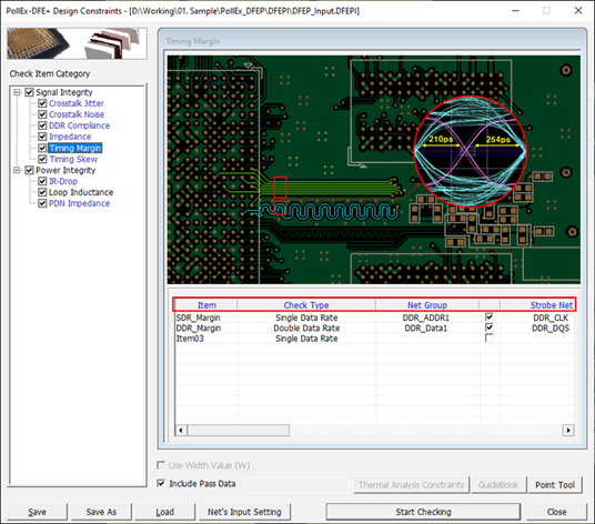
This item analyzes and checks setup/hold time margin of SDR/DDR memory
system.
The SDR means that the operating frequency of signal is half of the operating
frequency of strobe signal.
The DDR means that the operating frequency of signal is the same as the operating
frequency of strobe signal.
This item checks the followings:
The setup time margin of SDR/DDR memory system.
The hold time margin of SDR/DDR memory system. Figure 1.
Item: Sub item name. You can enter arbitrary name.
Check Type: Select the clock operation structure of the memory system.
Single Data Rate: Select if the operating frequency of signal is
half of the operating frequency of strobe signal.
Double Data Rate: Select if the operating frequency of signal is the
same as the operating frequency of strobe signal.
Net Group: Select target net groups to be tested. Allow multiple net
groups.
Strobe Net: Option to select target strobe net groups to be tested.(Clock,
DQS, and so on)
Start Component: Select component group to be used as signal driver.
Except Component: Select component group to be excluded. Allow multiple
component groups.
Period(nS): Enter operating period in nS unit.
The pulse period of input signal is automatically filled if user use
Import DDR Spec option.
Setup Time: Enter required setup time in nS unit.
The setup time of input signal is automatically filled if you use
Import DDR Spec option.
Hold Time: Enter required setup time in nS unit.
The hold time of input signal is automatically filled if user use
Import DDR Spec option.
Setup Margin: Enter minimum required setup time margin in nS unit.
Hold Margin: Enter minimum required hold time margin in nS unit.
Tolerance(%) option: Enter allowable tolerance of setup/hold time
margin.
Use Default Vth(Option): This option specifies the reference voltage for
timing checks.
Uncheck: Set Vref to 1/2 of Waveform swing amplitude.
Check: Use Vref declared in IBIS file as Threshold Voltage.
Bi-Directional(Option): This option specifies the signaling direction of the signal.
Uncheck: Check only the direction in which the Start Component is
the Driver.
Check: Check the direction of Start Component as Driver and
Receiver.
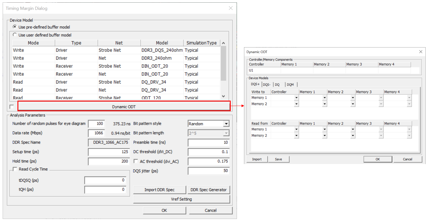
Analyze Options: You can assign driver/receiver buffer simulation model,
driving strength of driver and other simulation parameters.
There are two ways to assign the simulation buffer model:
Use pre-defined buffer model: The buffer model set in the electrical pin
part of UPE is used as default. The user cannot change the buffer model
here.
Use user defined buffer model: You can assign simulation buffer model.
The default buffer model is initially assigned to the buffer model field which can be
changed.
Click the Model field to view the device models selected for
the output and input pins. You can change the device model selection when multiple
models are available for the pin.
Prior to running analysis, you can change the analysis control parameters such as the
number of random pulses and bit pattern style. Figure 2.
Model: The default buffer model is initially assigned to the buffer model
field which can be changed by users. For the selected active driver, actual
driver model can be selectable among many different models in IBIS or Linear
device model types. User can use one of available models considering the
output impedance, driving capability measured by output current level and
operating frequencies. These driver’s characteristics lead huge impact on
the simulated waveforms.
Simulation Type: You can select the simulation type also among Typical,
Fast, and Slow. The simulation type is applied to all device models used for
the analysis.
Dynamic ODT: This function allows for the individual configuration of On-Die
Termination (ODT) for each memory when multiple memories are connected to a
single controller on a PCB.
Number of random pulses for eye diagram: Means the number of random pulses
excited to the simulating net during the eye diagram analysis.
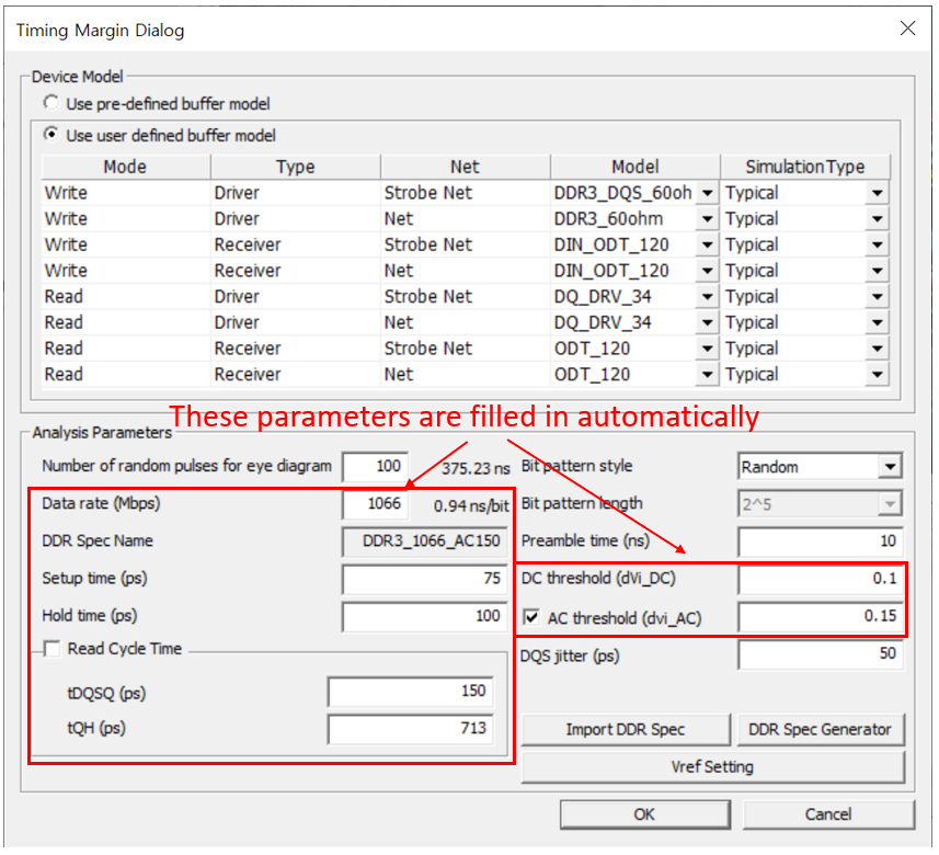
Clock speed (Mbps): Enter DDR BUS operating speed. This value is
automatically filled if user use Import DDR Spec option.
DDR Spec Name: Shows DDR specification name. This value is automatically
filled if user use Import DDR Spec option.
Setup time(pS): Enter required setup time. This value is automatically
filled if you use Import DDR Spec option.
Hold time(pS): Enter required hold time. This value is automatically filled
if you use Import DDR Spec option.
Bit pattern style: Select the numerical method among random, ABS (Artificial
Bit Stream) and PRBS (Pseudo Random Bit Stream) for generating the bit
sequences. ABS (Artificial Bit Stream) is a method designed to provide a
large pattern of bits to show worst case signal transmission quality of the
net that would quickly converge the eye diagram. PRBS (Pseudo Random Bit
Stream) is the mostly common method deemed as an industry standard.
Bit pattern length: If bit pattern style is ABS or PRBS, choose the bit
pattern length here.
Preamble time(pS): Enter this value. Simulation start after this time to
wait until status of internal circuit becomes stable.
DC threshold (dvi_DC): Enter threshold voltage value for hold time
measurement. This value is automatically filled if you use Import DDR Spec
option.
AC threshold (dvi_AC): Enter threshold voltage value for setup time
measurement. This value is automatically filled if you use Import DDR Spec
option.
Clock jitter(pS): Enter system DDR bus jitter value.
Read Cycle Time: Enter Read Cycle Time(tDQSQ, tQH) value for DQS time
measurement when the memory operates as read cycle. This value is
automatically filled if user use Import DDR Spec option.
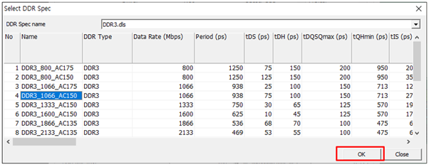
Import DDR Spec: In order to analyze DDR timing, enter every timing
parameter manually. Click Import DDR Spec to
automatically bring in a DDR timing specification to use among available DDR
timing tables. Figure 3. Figure 4.
DDR Spec Generator: You can also generate a new DDR timing specification
into the exist DDR timing tables.
Vref_DQ Setting: Normally the voltage level of Vref_DQ for timing check is
defined by specification. But some technology memories, such as DDR4,
require setting Vref_DQ value. Using this option, you assign Vref_DQ voltage
level.
Extract Vref_DQ using analysis result: Using this option, the DFE+ tool find
the appropriate Vref_DQ value during analysis.
Vref_DQ training result: You can assign Vref_DQ value for each memory
component manually.