Frequency Domain Parameter
This item analyzes 4 types of frequency domain parameter (S11, S21, S13, S14) using the standard s-parameter port numbering scheme and a signal is injected at port1.
This item checks following:
- Return Loss (S11): The single-ended return loss is recommended to be less than 15dB up to 3 times the Nyquist frequency
- Insertion Loss (S21): The single-ended insertion loss is recommended to stay within 0 to 10dB up to 3 times the Nyquist frequency of operation. For example, if the target frequency is 8Gbps (4GHz Nyquist), the single-ended insertion loss should stay under 10dB up to 12GHz
- Near-end Crosstalk(S31) and Far-end Crosstalk(S41) are recommended to be under 25dB for frequencies up to 3times the Nyquist.

- Item: Sub item name. User can enter arbitrary.
- Net Group: Select target net groups to be tested. Allow multiple net groups.
- Coupling Condition: Change the following coupling conditions. number of
coupling signal layers, number of traces to be coupled, coupling length,
distance, etc.
Figure 2. 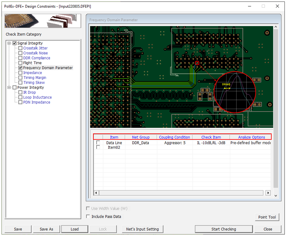
- Check Item:
- Insertion Loss Limit(dB): If Insertion Loss value is smaller than the limit value user entered, it fails.
- Return Path(dB): If Return Path value is bigger than the limit value user entered, it fails.
- Near-end Crosstalk Limit(dB): If NEXT value is smaller than the limit value user entered, it fails.
- Far-end Crosstalk Limit(dB): If FEXT value is smaller than the limit
value user entered, it fails.
Figure 3. 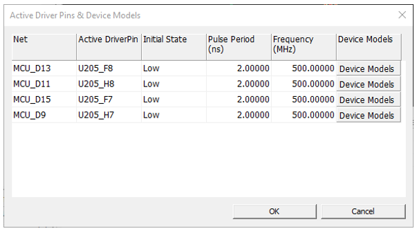
- Analyze Options :
- You can assign driver/receiver buffer simulation model, driving
strength of driver and other simulation parameters. The default
buffer model is initially assigned to the buffer model field which
can be changed. When the device models are not available in the part
data, the default linear device models defined here are used for
transient simulation of signal integrity analyses.
Figure 4. 
- You can assign driver/receiver buffer simulation model, driving
strength of driver and other simulation parameters. The default
buffer model is initially assigned to the buffer model field which
can be changed. When the device models are not available in the part
data, the default linear device models defined here are used for
transient simulation of signal integrity analyses.
- The region shows the names of all coupled nets. Total 7 aggressor nets listed together with the victim MCU_AA0 net.
- Display region shows detailed coupling topologies.
- Aggressor Net: Many fractal segments can be listed at this column coupled to the victim net.
- Separation: Aggressor net MCU_ABA2 can have different separations to the victim depending on the locations.
- Victim Layer: With Aggressor Layer, two columns show where the coupled traces, one is victim and the other is aggressor, are routed.
- Coupled Length: Shows the coupled length for the fractal coupled segments.
- Network Analysis Parameters: Enter required analysis parameter.
- Starting frequency(MHz): Start frequency for Network Parameter Analysis.
- Ending frequency(MHz): End frequency for Network Parameter Analysis.
- Frequency sweep type: Quadratic, Linear.
- Number of frequency point per decade: Specify the desired output saving frequencies.
- Default Device Models: When the device models are not available in the part data, the default linear device models defined here are used for transient simulation of signal integrity analyses. With the use of Linear Device Modeler, you can create linear output (driver) and input (receiver) device models and store them in a linear device model file. PollEx DFE+ provides users with a system default linear device model file, UDVS.dmf.
- Active Driver Pins & Device Models: Click then Active Driver Pins &
Device Models dialog is invoked. You can define whether the excitation
signal is applied or not for each aggressor nets here. During crosstalk
jitter analysis, the Active Driver Pin of victim net also set as drive. Just
do the crosstalk analysis with all aggressor and victim nets are excited.
User can change the Initial State, Pulse Period(ns) and Device Models by
clicking these for the desired net. When testing Crosstalk Jitter, both
Victim and Aggressor are in driving mode.
Figure 5. 